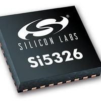
SI5326C-B-GM Silicon Laboratories Inc, SI5326C-B-GM Datasheet - Page 9

SI5326C-B-GM
Manufacturer Part Number
SI5326C-B-GM
Description
IC ANY-RATE MULTI/ATTEN 36QFN
Manufacturer
Silicon Laboratories Inc
Type
Clock Multiplierr
Specifications of SI5326C-B-GM
Number Of Circuits
1
Package / Case
36-QFN
Pll
Yes
Input
Clock
Output
CML, CMOS, LVDS, LVPECL
Ratio - Input:output
2:2
Differential - Input:output
Yes/Yes
Frequency - Max
346MHz
Divider/multiplier
Yes/Yes
Voltage - Supply
1.62 V ~ 3.63 V
Operating Temperature
-40°C ~ 85°C
Mounting Type
Surface Mount
Frequency-max
346MHz
Maximum Input Frequency
710 MHz
Minimum Input Frequency
0.002 MHz
Output Frequency Range
0.002 MHz to 1400 MHz
Supply Voltage (max)
3.63 V
Supply Voltage (min)
1.71 V
Maximum Operating Temperature
+ 85 C
Minimum Operating Temperature
- 40 C
Mounting Style
SMD/SMT
Operating Supply Voltage
1.8 V, 2.5 V, 3.3 V
Lead Free Status / RoHS Status
Lead free / RoHS Compliant
Note: Internal register names are indicated by underlined italics, e.g. INT_PIN. See Si5326 Register Map.
Pin #
19
20
21
22
Pin Name
CS_CA
DEC
SCL
INC
I/O
I/O
I
I
I
Signal Level
LVCMOS
LVCMOS
LVCMOS
LVCMOS
Confidential Rev. 0.2
Latency Decrement.
A pulse on this pin decreases the input to output device latency by
1/f
latency adjustment by this method.
Pin control is enabled by setting INCDEC_PIN = 1. If
INCDEC_PIN = 0, this pin is ignored and output latency is con-
trolled via the CLAT register.
If both INC and DEC are tied high, phase buildout is disabled and
the device maintains a fixed-phase relationship between the
selected input clock and the output clock during an input clock
switch.
This pin has a weak pull-down.
Latency Increment.
A pulse on this pin increases the input to output device latency by
1/f
latency adjustment by this method.
Pin control is enabled by setting INCDEC_PIN = 1. If
INCDEC_PIN = 0, this pin is ignored and output latency is con-
trolled via the CLAT register.
If both INC and DEC are tied high, phase buildout is disabled and
the device maintains a fixed-phase relationship between the
selected input clock and the output clock during an input clock
switch.
This pin has a weak pull-down.
Input Clock Select/Active Clock Indicator.
In manual clock selection mode, this pin functions as the manual
input clock selector if the CKSEL_PIN is set to 1.
0 = Select CKIN1.
1 = Select CKIN2.
If CKSEL_PIN = 0, the CKSEL_REG register bit controls this func-
tion and this input tristates.
In automatic clock selection mode, this pin indicates which of the
two input clocks is currently the active clock. If alarms exist on both
clocks, CK_ACTV will indicate the last active clock that was used
before entering the digital hold state. The CK_ACTV_PIN register
bit must be set to 1 to reflect the active clock status to the
CK_ACTV output pin.
0 = CKIN1 active input clock.
1 = CKIN2 active input clock.
If CK_ACTV_PIN = 0, this pin will tristate. The CK_ACTV status
will always be reflected in the CK_ACTV_REG read only register
bit.
This pin has a weak pull-down.
Serial Clock/Serial Clock.
This pin functions as the serial clock input for both SPI and I
modes.
OSC
OSC
(approximately 200 ps). There is no limit on the range of
(approximately 200 ps). There is no limit on the range of
Description
Si5326
2
C
9


