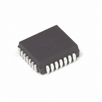
MC88915FN70R2 Freescale Semiconductor, MC88915FN70R2 Datasheet - Page 4

MC88915FN70R2
Manufacturer Part Number
MC88915FN70R2
Description
IC DRIVER CLK PLL 70MHZ 28-PLCC
Manufacturer
Freescale Semiconductor
Type
Clock Driver, Fanout Distribution, Multiplexerr
Datasheet
1.MC88915FN55.pdf
(13 pages)
Specifications of MC88915FN70R2
Pll
Yes
Input
TTL
Output
CMOS, TTL
Number Of Circuits
1
Ratio - Input:output
3:8
Differential - Input:output
No/No
Frequency - Max
70MHz
Divider/multiplier
Yes/Yes
Voltage - Supply
4.75 V ~ 5.25 V
Operating Temperature
0°C ~ 70°C
Mounting Type
Surface Mount
Package / Case
28-PLCC
Frequency-max
70MHz
Lead Free Status / RoHS Status
Contains lead / RoHS non-compliant
Other names
MC88915FN70R2TR
Available stocks
Company
Part Number
Manufacturer
Quantity
Price
Company:
Part Number:
MC88915FN70R2
Manufacturer:
MOTOROLA
Quantity:
268
Company:
Part Number:
MC88915FN70R2
Manufacturer:
Freescale Semiconductor
Quantity:
10 000
Part Number:
MC88915FN70R2
Manufacturer:
MOTOROLA/摩托罗拉
Quantity:
20 000
MC88915
AC ELECTRICAL CHARACTERISTICS (T A =0 C to +70 C, V CC = 5.0V 5%, C L = 50pF)
1. Under equally loaded conditions, C L 50pF ( 2pF), and at a fixed temperature and voltage.
2. With V CC fully powered–on and an output properly connected to the FEEDBACK pin. t LOCK Max. is with C1 = 0.1 F, t LOCK Min is with
3. These specifications are not tested, they are guaranteed by statistical characterization. See General AC Specification note 1.
RESET TIMING REQUIREMENTS
1. These reset specs are valid only when PLL_EN is LOW and the part is in Test mode (not in phase–lock)
(Sync–Feedback)
MOTOROLA
(Q0,Q1,Q3,Q4,
t RISE , t FALL 3
(2X_Q Output)
(2X_Q Output)
(2X_Q Output)
t Pulse Width 3
t Pulse Width 3
t Pulse Width 3
t Pulse Width 3
C1 = 0.01 F.
t RISE , t FALL
t SKEWall 1,3
t SKEWr 1,3
t SKEWf 1,3
(Reset – Q)
(Outputs)
(Q2 only)
Symbol
(Falling)
Q5,Q/2)
(Rising)
t LOCK
t PD 3
t PHL
t REC , RST
to SYNC
t W , RST
Symbol
LOW
Rise and Fall Times, all Outputs Into a 50 pF, 500
(Between 0.2V CC and 0.8V CC )
Rise and Fall Time, 2X_Q Output Into a 20 pF Load With Termina-
tion specified in note 2 (Between 0.8 V and 2.0 V)
Output Pulse Width (Q0, Q1, Q3, Q4, Q5, Q/2 @V CC /2)
Output Pulse Width (Q2 Output @ V CC /2)
Output Pulse Width (2X_Q Output @ 1.5 V) (See AC Note 2)
Output Pulse Width (2X_Q Output @ V CC /2)
SYNC input to feedback delay
(meas. @ SYNC0 or 1 and FEEDBACK input pins)
(See General AC Specification note 4 and Fig. 2 for explanation)
Output–to–Output Skew Between Outputs Q0 – Q4, Q/2
(Rising Edges Only)
Output–to–Output Skew Between Outputs Q0 – Q4
(Falling Edges Only)
Output–to–Output Skew Between Outputs 2X_Q, Q/2, Q0 – Q4
Rising, Q5 Falling
Time Required to acquire 2 Phase–Lock from time SYNC Input Sig-
nal is Received.
Propagation Delay, RST to Any Output (High–Low)
Reset Recovery Time rising RST
1
edge to falling SYNC edge
Minimum Pulse Width,
RST input LOW
Parameter
Parameter
4
Load
Minimum
9.0
5.0
0.5t CYCLE – 0.5
0.5t CYCLE – 0.6
0.5t CYCLE – 0.5
0.5t CYCLE – 1.0
t CYCLE = 1/Freq. at which the “Q”
(470k From RC1 to An.GND)
(470k From RC1 to An.V CC )
–1.05
+1.25
Min
1.0
0.5
1.5
–
–
–
1
Outputs are running
0.5t CYCLE + 0.5
0.5t CYCLE + 0.6
0.5t CYCLE + 0.5
0.5t CYCLE + 1.0
–0.50
+3.25
TIMING SOLUTIONS
Max
13.5
500
750
750
2.5
1.6
10
Unit
ns
ns
BR1333 — Rev 6
Unit
ms
ns
ns
ns
ns
ns
ns
ps
ps
ps
ns


