LMX2336USLBX National Semiconductor, LMX2336USLBX Datasheet - Page 8
LMX2336USLBX
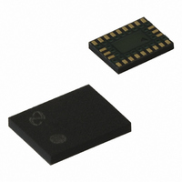
Manufacturer Part Number
LMX2336USLBX
Description
IC FREQ SYNTH DUAL 24LAMINATECSP
Manufacturer
National Semiconductor
Series
PLLatinum™r
Type
PLL Frequency Synthesizerr
Datasheet
1.LMX2335UTMNOPB.pdf
(48 pages)
Specifications of LMX2336USLBX
Pll
Yes with Bypass
Input
CMOS, TTL
Output
CMOS
Number Of Circuits
1
Ratio - Input:output
3:1
Differential - Input:output
Yes/No
Frequency - Max
2GHz, 1.2GHz
Divider/multiplier
Yes/No
Voltage - Supply
2.7 V ~ 5.5 V
Operating Temperature
-40°C ~ 85°C
Mounting Type
Surface Mount
Package / Case
24-Laminate CSP
Frequency-max
2GHz
Lead Free Status / RoHS Status
Contains lead / RoHS non-compliant
Other names
LMX2336USLBXTR


www.national.com
I
I
I
I
I
RF1 SYNTHESIZER PARAMETERS
f
N
R
F
Pf
CC
CC RF1 + RF2
CC RF1
CC RF2
CC-PWDN
IN
φRF1
RF1
RF1
Absolute Maximum Ratings
2, 3)
If Military/Aerospace specified devices are required,
please contact the National Semiconductor Sales Office/
Distributors for availability and specifications.
Electrical Characteristics
V
IN
Symbol
Power Supply Voltage
Voltage on any pin to GND (V
Storage Temperature Range (T
Lead Temperature (solder 4 s) (T
16-Pin TSSOP θ
Impedance
20-Pin TSSOP θ
Impedance
RF1
CC
PARAMETERS
RF1
V
V
V
V
CC
P
P
I
= V
must be
RF1 to GND
RF2 to GND
to GND
P
RF1 = V
Power Supply
Current, RF1 + RF2
Synthesizers
Power Supply
Current, RF1
Synthesizer Only
Power Supply
Current, RF2
Synthesizer Only
Powerdown Current
RF1 Operating
Frequency
RF1 N Divider Range
RF1 R Divider Range
RF1 Phase Detector Frequency
RF1 Input Sensitivity
<
+6.5V
JA
JA
P
Thermal
Thermal
RF2 = 3.0V, −40˚C ≤ T
Parameter
I
)
S
)
L
)
LMX2335U
LMX2336U
LMX2335U
LMX2336U
LMX2335U
LMX2336U
LMX2335U/
LMX2336U
LMX2335U
LMX2336U
−0.3V to V
−65˚C to +150˚C
−0.3V to +6.5V
−0.3V to +6.5V
−0.3V to +6.5V
A
≤ +85˚C, unless otherwise specified
(Notes 1,
137.1˚C/W
114.5˚C/W
CC
+260˚C
Clock, Data and LE = GND
OSC
PWDN RF1 Bit = 0
PWDN RF2 Bit = 0
Clock, Data and LE = GND
OSC
PWDN RF1 Bit = 0
PWDN RF2 Bit = 1
Clock, Data and LE = GND
OSC
PWDN RF1 Bit = 1
PWDN RF2 Bit = 0
Clock, Data and LE = GND
OSC
PWDN RF1 Bit = 1
PWDN RF2 Bit = 1
Prescaler = 64/65
(Note 4)
Prescaler = 128/129
(Note 4)
2.7V ≤ V
(Note 5)
3.0V
(Note 5)
+0.3V
in
in
in
in
<
= GND
= GND
= GND
= GND
V
CC
CC
8
≤ 3.0V
Conditions
≤ 5.5V
Recommended Operating
Conditions
Note 1: Absolute Maximum Ratings indicate limits beyond which damage to
the device may occur. Recommended Operating Conditions indicate condi-
tions for which the device is intended to be functional, but do not guarantee
specific performance limits. For guaranteed specifications and test condi-
tions, see the Electrical Characteristics. The guaranteed specifications apply
only for the test conditions listed.
Note 2: This device is a high performance RF integrated circuit with an ESD
rating
should only be done at ESD protected work stations.
Note 3: GND = 0V
16-Pin CSP θ
24-Pin CSP θ
Power Supply Voltage
Operating Temperature (T
V
V
V
CC
P
P
<
RF1 to GND
RF2 to GND
2 kV and is ESD sensitive. Handling and assembly of this device
to GND
JA
JA
Thermal Impedance
Thermal Impedance
(Note 1)
Min
100
200
192
384
−15
−10
3
A
)
Value
Typ
3.0
3.5
1.5
2.0
1.5
1.5
1.0
−40˚C to +85˚C
+2.7V to +5.5V
V
V
131135
262143
32767
CC
CC
1200
2000
Max
10.0
4.0
4.5
2.0
2.5
2.0
2.0
10
0
0
130˚C/W
112˚C/W
to +5.5V
to +5.5V
Units
MHz
MHz
MHz
dBm
dBm
mA
mA
mA
mA
mA
µA
Related parts for LMX2336USLBX
Image
Part Number
Description
Manufacturer
Datasheet
Request
R

Part Number:
Description:
PLLatinum Ultra Low Power Dual Frequency Synthesizer for RF Personal Communications
Manufacturer:
NSC [National Semiconductor]
Datasheet:

Part Number:
Description:
National Semiconductor [8-Bit D/A Converter]
Manufacturer:
National Semiconductor
Datasheet:
Part Number:
Description:
National Semiconductor [Media Coprocessor]
Manufacturer:
National Semiconductor
Datasheet:
Part Number:
Description:
Digitally Controlled Tone and Volume Circuit with Stereo Audio Power Amplifier, Microphone Preamp Stage and National 3D Sound
Manufacturer:
National Semiconductor
Datasheet:
Part Number:
Description:
Digitally Controlled Tone and Volume Circuit with Stereo Audio Power Amplifier, Microphone Preamp Stage and National 3D Sound
Manufacturer:
National Semiconductor
Datasheet:
Part Number:
Description:
AC97 Rev 2 Codec with Sample Rate Conversion and National 3D Sound
Manufacturer:
National Semiconductor
Part Number:
Description:
Manufacturer:
National Semiconductor
Datasheet:
Part Number:
Description:
Manufacturer:
National Semiconductor
Datasheet:
Part Number:
Description:
General Purpose, Low Voltage, Low Power, Rail-to-Rail Output Operational Amplifiers
Manufacturer:
National Semiconductor
Datasheet:
Part Number:
Description:
8-bit 20 MSPS flash A/D converter.
Manufacturer:
National Semiconductor
Datasheet:
Part Number:
Description:
Low Noise Quad Operational Amplifier
Manufacturer:
National Semiconductor
Datasheet:
Part Number:
Description:
Quad Differential Line Receivers
Manufacturer:
National Semiconductor
Datasheet:
Part Number:
Description:
Quad High Speed Trapezoidal? Bus Transceiver
Manufacturer:
National Semiconductor
Datasheet:
Part Number:
Description:
Dual Line Receiver
Manufacturer:
National Semiconductor
Datasheet: