LMX2336USLBX National Semiconductor, LMX2336USLBX Datasheet - Page 34
LMX2336USLBX
Manufacturer Part Number
LMX2336USLBX
Description
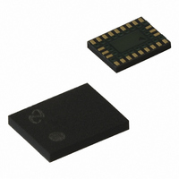
IC FREQ SYNTH DUAL 24LAMINATECSP
Manufacturer
National Semiconductor
Series
PLLatinum™r
Type
PLL Frequency Synthesizerr
Datasheet
1.LMX2335UTMNOPB.pdf
(48 pages)
Specifications of LMX2336USLBX
Pll
Yes with Bypass
Input
CMOS, TTL
Output
CMOS
Number Of Circuits
1
Ratio - Input:output
3:1
Differential - Input:output
Yes/No
Frequency - Max
2GHz, 1.2GHz
Divider/multiplier
Yes/No
Voltage - Supply
2.7 V ~ 5.5 V
Operating Temperature
-40°C ~ 85°C
Mounting Type
Surface Mount
Package / Case
24-Laminate CSP
Frequency-max
2GHz
Lead Free Status / RoHS Status
Contains lead / RoHS non-compliant
Other names
LMX2336USLBXTR


www.national.com
1.0 Functional Description
1.5 PHASE/FREQUENCY DETECTORS
The RF1 and RF2 phase/frequency detectors are driven
from their respective N and R counter outputs. The maxi-
mum frequency for both the RF1 and RF2 phase detector
inputs is 10 MHz. The phase/frequency detector outputs
control the respective charge pumps. The polarity of the
pump-up or pump-down control signals are programmed
using the PD_POL RF1 or PD_POL RF2 control bits, de-
PHASE COMPARATOR AND INTERNAL CHARGE PUMP CHARACTERISTICS
1.6 CHARGE PUMPS
The charge pump directs charge into or out of an external
loop filter. The loop filter converts the charge into a stable
control voltage which is applied to the tuning input of the
VCO. The charge pump steers the VCO control voltage
towards V
towards GND during pump-down events. When locked, D
RF1 or D
corrections occuring at the phase comparator rate. The
charge pump output current magnitude can be selected by
toggling the ID
1.7 MICROWIRE SERIAL INTERFACE
The programmable register set is accessed via the MI-
CROWIRE serial interface. The interface is comprised of
three signal pins: Clock, Data and LE (Latch Enable). Serial
data is clocked into the 22-bit shift register on the rising edge
of Clock. The last two bits decode the internal control regis-
ter address. When LE transitions HIGH, data stored in the
shift register is loaded into one of four control registers
depending on the state of the address bits. The MSB of Data
is loaded in first. The synthesizers can be programmed even
in power down mode. A complete programming description
is provided in Section 2.0 Programming Description.
Notes:
1.
2.
3.
4.
5.
o
RF2 are primarily in a TRI-STATE mode with small
P
The minimum width of the pump-up and pump-down current pulses occur at the D
The diagram assumes positive VCO characteristics, i.e. PD_POL RF1 or PD_POL RF2 = 1.
F
F
D
r
p
o
RF1 or V
is the phase detector input from the reference divider (R counter).
is the phase detector input from the programmable feedback divder (N counter).
refers to either the RF1 or RF2 charge pump output.
o
RF1 or ID
P
RF2 during pump-up events and
o
RF2 control bits.
(Continued)
o
34
pending on whether the RF1 or RF2 VCO characteristics are
positive or negative. Refer to Sections 2.4.2 and 2.6.2 for
more details. The phase/frequency detectors have a detec-
tion range of −2π to +2π. The phase/frequency detectors
also receive a feedback signal from the charge pump in
order to eliminate dead zone.
1.8 MULTI-FUNCTION OUTPUTS
The F
configured as the RF1 FastLock output, a push-pull analog
lock detect output, counter reset, or used to monitor the
output of the various reference divider (R counter) or feed-
back divider (N counter) circuits. The F
used to select the desired output function. When the PLL is
in powerdown mode, the F
state. A complete
multi-function output is provided in Section 2.8 F
1.8.1 Push-Pull Analog Lock Detect Output
An analog lock detect status generated from the phase
detector is available on the F
lock detect output goes HIGH when the charge pump is
inactive. It goes LOW when the charge pump is active during
a comparison cycle. When viewed with an oscilloscope,
narrow negative pulses are observed when the charge pump
turns on. The lock detect output signal is a push-pull con-
figuration.
Three separate lock detect signals are routed to the multi-
plexer. Two of these monitor the ‘lock’ status of the individual
synthesizers. The third detects the condition when both the
RF1 and RF2 synthesizers are in a ‘locked state’. External
circuitry however, is required to provide a steady DC signal
to indicate when the PLL is in a locked state. Refer to
Section 2.8 F
lock detect options.
o
LD output pin is a multi-function output that can be
o
RF1 or D
o
LD for details on how to program the different
o
RF2 pins when the loop is phase locked.
programming
o
LD output is pulled to a LOW
o
LD output pin if selected. The
10136785
description
o
LD control word is
o
LD.
of
the
Related parts for LMX2336USLBX
Image
Part Number
Description
Manufacturer
Datasheet
Request
R

Part Number:
Description:
PLLatinum Ultra Low Power Dual Frequency Synthesizer for RF Personal Communications
Manufacturer:
NSC [National Semiconductor]
Datasheet:

Part Number:
Description:
National Semiconductor [8-Bit D/A Converter]
Manufacturer:
National Semiconductor
Datasheet:
Part Number:
Description:
National Semiconductor [Media Coprocessor]
Manufacturer:
National Semiconductor
Datasheet:
Part Number:
Description:
Digitally Controlled Tone and Volume Circuit with Stereo Audio Power Amplifier, Microphone Preamp Stage and National 3D Sound
Manufacturer:
National Semiconductor
Datasheet:
Part Number:
Description:
Digitally Controlled Tone and Volume Circuit with Stereo Audio Power Amplifier, Microphone Preamp Stage and National 3D Sound
Manufacturer:
National Semiconductor
Datasheet:
Part Number:
Description:
AC97 Rev 2 Codec with Sample Rate Conversion and National 3D Sound
Manufacturer:
National Semiconductor
Part Number:
Description:
Manufacturer:
National Semiconductor
Datasheet:
Part Number:
Description:
Manufacturer:
National Semiconductor
Datasheet:
Part Number:
Description:
General Purpose, Low Voltage, Low Power, Rail-to-Rail Output Operational Amplifiers
Manufacturer:
National Semiconductor
Datasheet:
Part Number:
Description:
8-bit 20 MSPS flash A/D converter.
Manufacturer:
National Semiconductor
Datasheet:
Part Number:
Description:
Low Noise Quad Operational Amplifier
Manufacturer:
National Semiconductor
Datasheet:
Part Number:
Description:
Quad Differential Line Receivers
Manufacturer:
National Semiconductor
Datasheet:
Part Number:
Description:
Quad High Speed Trapezoidal? Bus Transceiver
Manufacturer:
National Semiconductor
Datasheet:
Part Number:
Description:
Dual Line Receiver
Manufacturer:
National Semiconductor
Datasheet: