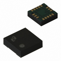
LMX2335USLBX National Semiconductor, LMX2335USLBX Datasheet - Page 35

LMX2335USLBX
Manufacturer Part Number
LMX2335USLBX
Description
IC FREQ SYNTH DUAL 16LAMINATECSP
Manufacturer
National Semiconductor
Series
PLLatinum™r
Type
PLL Frequency Synthesizerr
Datasheet
1.LMX2335UTMNOPB.pdf
(48 pages)
Specifications of LMX2335USLBX
Pll
Yes with Bypass
Input
CMOS, TTL
Output
CMOS
Number Of Circuits
1
Ratio - Input:output
3:1
Differential - Input:output
No/No
Frequency - Max
1.2GHz
Divider/multiplier
Yes/No
Voltage - Supply
2.7 V ~ 5.5 V
Operating Temperature
-40°C ~ 85°C
Mounting Type
Surface Mount
Package / Case
16-Laminate CSP
Frequency-max
1.2GHz
Lead Free Status / RoHS Status
Contains lead / RoHS non-compliant
Other names
LMX2335USLBXTR
1.0 Functional Description
1.8.2 Open Drain FastLock Output
The LMX233xU Fastlock feature allows faster loop response
time during lock aquisition. The loop response time (lock
time) can be approximately halved if the loop bandwidth is
doubled. In order to achieve this, the same gain/ phase
relationship at twice the loop bandwidth must be maintained.
This can be achieved by increasing the charge pump current
from 0.95 mA (ID
3.8 mA (ID
is configured as a FastLock output, an open drain device is
enabled. The open drain device switches in a parallel resis-
tor R2’ to ground, of equal value to resistor R2 of the external
loop filter. The loop bandwidth is effectively doubled and
stability is maintained. Once locked to the correct frequency,
the PLL will return to a steady state condition. Refer to
Section 2.8 F
output to an open drain Fastlock output.
1.8.3 Counter Reset
Three separate counter reset functions are provided. When
the F
RF2 feedback divider and the RF2 reference divider are held
at their load point. When the Reset RF1 Counters is pro-
grammed, both the RF1 feedback divider and the RF1 ref-
erence divider are held at their load point. When the Reset
All Counters mode is enabled, all feedback dividers and
reference dividers are held at their load point. When the
device is programmed to normal operation, both the feed-
back divider and reference divider are enabled and resume
counting in ‘close’ alignment to each other. Refer to Section
2.8 F
1.8.4 Reference Divider and Feedback Divider Output
The outputs of the various N and R dividers can be moni-
tored by selecting the appropriate F
tial when performing OSC
Refer to the Test Setups section for more details. Refer to
Section 2.8 F
appropriate divider output to the F
Notes:
1. TRI-STATE ID
2. PWDN refers to either the PWDN RF1 or PWDN RF2 bit.
TRI-STATE ID
o
o
LD is programmed to Reset RF2 Counters, both the
LD for more details.
o
0
1
0
1
RF1 Bit = 1) in Fastlock. When the F
o
o
LD for details on how to configure the F
LD for more details on how to route the
o
o
o
refers to either the TRI-STATE ID
RF1 Bit = 0) in the steady state mode, to
in
or f
IN
sensitivity measurements.
o
o
LD pin.
LD word. This is essen-
PWDN
0
0
1
1
(Continued)
o
LD output
o
RF1 or TRI-STATE ID
o
LD
PLL Active, Normal Operation
PLL Active, Charge Pump Output in High Impedance State
Synchronous Powerdown
Asynchronous Powerdown
35
1.9 POWER CONTROL
Each synthesizer in the LMX2335U or LMX2336U is indi-
vidually power controlled by device powerdown bits. The
powerdown word is comprised of the PWDN RF1 (PWDN
RF2) bit, in conjuction with the TRI-STATE ID
(TRI-STATE ID
used to set the operating mode of the device. Refer to
Sections 2.4.4, 2.5.4, 2.6.4, and 2.7.4 for details on how to
program the RF1 or RF2 powerdown bits.
When either the RF1 synthesizer or the RF2 synthesizer
enters the powerdown mode, the respective prescaler,
phase detector, and charge pump circuit are disabled. The
D
pins are all forced to a high impedance state. The reference
divider and feedback divider circuits are held at the load
point during powerdown. The oscillator buffer is disabled
when both the RF1 and RF2 synthesizers are powered
down. The OSC
approximate 100 kΩ resistance when this condition exists.
When either synthesizer is activated, the respective pres-
caler, phase detector, charge pump circuit, and the oscillator
buffer are all powered up. The feedback divider, and the
reference divider are held at load point. This allows the
reference oscillator, feedback divider, reference divider and
prescaler circuitry to reach proper bias levels. After a finite
delay, the feedback and reference dividers are enabled and
they resume counting in ‘close’ alignment (the maximum
error is one prescaler cycle). The MICROWIRE control reg-
ister remains active and capable of loading and latching data
while in the powerdown mode.
Synchronous Powerdown Mode
In this mode, the powerdown function is gated by the charge
pump. When the device is configured for synchronous pow-
erdown, the device will enter the powerdown mode upon
completion of the next charge pump pulse event.
Asynchronous Powerdown Mode
In this mode, the powerdown function is NOT gated by the
completion of a charge pump pulse event. When the device
is configured for asynchronous powerdown, the part will go
into powerdown mode immediately.
o
RF1 (D
o
RF2 bit .
o
RF2), f
o
in
Operating Mode
RF2) bit. The powerdown control word is
pin is forced to a HIGH state through an
IN
RF1 (f
IN
RF2), and f
IN
RF1 (f
www.national.com
IN
o
RF2)
RF1


