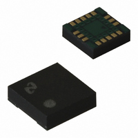
LMX2335USLBX National Semiconductor, LMX2335USLBX Datasheet - Page 12

LMX2335USLBX
Manufacturer Part Number
LMX2335USLBX
Description
IC FREQ SYNTH DUAL 16LAMINATECSP
Manufacturer
National Semiconductor
Series
PLLatinum™r
Type
PLL Frequency Synthesizerr
Datasheet
1.LMX2335UTMNOPB.pdf
(48 pages)
Specifications of LMX2335USLBX
Pll
Yes with Bypass
Input
CMOS, TTL
Output
CMOS
Number Of Circuits
1
Ratio - Input:output
3:1
Differential - Input:output
No/No
Frequency - Max
1.2GHz
Divider/multiplier
Yes/No
Voltage - Supply
2.7 V ~ 5.5 V
Operating Temperature
-40°C ~ 85°C
Mounting Type
Surface Mount
Package / Case
16-Laminate CSP
Frequency-max
1.2GHz
Lead Free Status / RoHS Status
Contains lead / RoHS non-compliant
Other names
LMX2335USLBXTR
www.national.com
PHASE NOISE CHARACTERISTICS
L
L(f) RF2
N
Electrical Characteristics
V
Note 4: Some of the values in this range are illegal divide ratios (B
≥ P
Note 5: Refer to the LMX2335U and LMX2336U f
Note 6: Refer to the LMX2335U and LMX2336U Charge Pump Test Setup section
Note 7: Refer to the Charge Pump Current Specification Definitions for details on how these measurements are made.
Note 8: Refer to the LMX2335U and LMX2336U OSC
Note 9: Refer to the LMX2335U and LMX2336U Serial Data Input Timing section
Note 10: Normalized Phase Noise Contribution is defined as : L
measured at an offset frequency, f, in a 1 Hz bandwidth. The offset frequency, f, must be chosen sufficiently smaller than the PLL’s loop bandwidth, yet large enough
to avoid substantial phase noise contribution from the reference source. N is the value selected for the feedback divider and F
comparison frequency..
Note 11: The synthesizer phase noise is measured with the LMX2335TMEB/LMX2335SLBEB or LMX2336TMEB/LMX2336SLBEB/LMX2336SLEEB Evaluation
boards and the HP8566B Spectrum Analyzer.
Symbol
(f) RF2
CC
*
(P−1), where P is the value selected for the prescaler.
= V
P
RF1 = V
RF2 Synthesizer Normalized Phase
Noise Contribution
(Note 10)
RF2 Synthesizer
Single Side Band
Phase Noise
Measured
P
RF2 = 3.0V, −40˚C ≤ T
Parameter
LMX2335U
LMX2336U
IN
Sensitivity Test Setup section
in
(Continued)
A
Sensitivity Test Setup section
≤ +85˚C, unless otherwise specified
N
TCXO Reference Source
ID
f
f = 1 kHz Offset
F
Loop Bandwidth = 12 kHz
N = 4500
F
V
ID
PWDN RF1 Bit = 1
T
(Note 11)
f
f = 1 kHz Offset
F
Loop Bandwidth = 12 kHz
N = 4500
F
V
ID
PWDN RF1 Bit = 1
T
(Note 11)
(f) = L(f) − 20 log (N) − 10 log (F
IN
IN
<
φRF2
OSC
A
φRF2
OSC
A
OSC
OSC
o
o
o
A). To obtain continuous legal division, the Minimum Divide Ratio must be calculated. Use N
RF2 = 900 MHz
RF2 = 900 MHz
= +25˚C
= +25˚C
RF2 Bit = 1
RF2 Bit = 1
RF2 Bit = 1
= 10 MHz
= 10 MHz
= 0.632 V
= 0.632 V
= 200 kHz
= 200 kHz
12
Conditions
PP
PP
φ
), where L(f) is defined as the single side band phase noise
Min
φ
is the RF1/RF2 phase detector
-212.0
-85.94
-85.94
Value
Typ
Max
Units
dBc/
dBc/
dBc/
Hz
Hz
Hz


