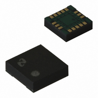
LMX2335USLBX National Semiconductor, LMX2335USLBX Datasheet - Page 28

LMX2335USLBX
Manufacturer Part Number
LMX2335USLBX
Description
IC FREQ SYNTH DUAL 16LAMINATECSP
Manufacturer
National Semiconductor
Series
PLLatinum™r
Type
PLL Frequency Synthesizerr
Datasheet
1.LMX2335UTMNOPB.pdf
(48 pages)
Specifications of LMX2335USLBX
Pll
Yes with Bypass
Input
CMOS, TTL
Output
CMOS
Number Of Circuits
1
Ratio - Input:output
3:1
Differential - Input:output
No/No
Frequency - Max
1.2GHz
Divider/multiplier
Yes/No
Voltage - Supply
2.7 V ~ 5.5 V
Operating Temperature
-40°C ~ 85°C
Mounting Type
Surface Mount
Package / Case
16-Laminate CSP
Frequency-max
1.2GHz
Lead Free Status / RoHS Status
Contains lead / RoHS non-compliant
Other names
LMX2335USLBXTR
www.national.com
Test Setups
The block diagram above illustrates the setup required to
measure the LMX2336U device’s RF1 charge pump sink
current. The same setup is used for the LMX2336TMEB/
LMX2336SLEEB Evaluation Boards. The RF2 charge pump
measurement setup is similar to the RF1 charge pump mea-
surement setup. The purpose of this test is to assess the
functionality of the RF1 charge pump.
This setup uses an open loop configuration. A power supply
is connected to V
of a signal generator, a 10 MHz signal is typically applied to
the f
detector. The 3 dB pad provides a 50 Ω match between the
PLL and the signal generator. The OSC
This establishes the other input to the phase detector. Alter-
natively, this input can be tied directly to the ground plane.
With the D
eter Analyzer in this way, the sink, source, and TRI-STATE
currents can be measured by simply toggling the Phase
Detector Polarity and Charge Pump State states in Code
Loader. Similarly, the LOW and HIGH currents can be mea-
sured by switching the Charge Pump Gain’s state between
1X and 4X in Code Loader.
IN
RF1 pin. The signal is one of two inputs to the phase
o
RF1 pin connected to a Semiconductor Param-
cc
and swept from 2.7V to 5.5V. By means
LMX2335U and LMX2336U Charge Pump Test Setup
in
pin is tied to V
cc
.
28
Let F
OSC
represent the frequency of the signal applied to the f
pin. The phase detector is sensitive to the rising edges of F
and F
pump turns ON and sinks current when the first rising edge
of F
pump continues to sink current indefinitely.
Toggling the Phase Detector Polarity state to negative
VCO characteristics allows the measurement of the RF1
charge pump source current. Likewise, selecting TRI-STATE
(TRI-STATE ID
Code Loader facilitates the measurement of the TRI-STATE
current.
The measurements are repeated at different temperatures,
namely T
The LMX2335U charge pump test setup is very much similar
to the above test setup.
p
in
r
p
is detected. Since F
represent the frequency of the signal applied to the
pin, which is simply zero in this case (DC), and let F
. Assuming positive VCO characteristics; the charge
A
= -40˚C, +25˚C, and +85˚C.
o
RF1 Bit = 1) for Charge Pump State in
r
has no rising edge, the charge
10136750
IN
RF1
p
r


