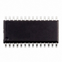
TDA7427AD1 STMicroelectronics, TDA7427AD1 Datasheet - Page 11

TDA7427AD1
Manufacturer Part Number
TDA7427AD1
Description
IC SYNTHESIZER/IF COUNTER SO-28
Manufacturer
STMicroelectronics
Type
PLL Frequency Synthesizerr
Datasheet
1.TDA7427AD1.pdf
(21 pages)
Specifications of TDA7427AD1
Pll
Yes
Input
Clock, Crystal
Output
Clock, Crystal
Number Of Circuits
1
Ratio - Input:output
3:1
Differential - Input:output
No/No
Frequency - Max
290MHz
Divider/multiplier
Yes/No
Voltage - Supply
4.5 V ~ 11 V
Operating Temperature
-40°C ~ 85°C
Mounting Type
Surface Mount
Package / Case
28-SOIC (7.5mm Width)
Frequency-max
290MHz
Lead Free Status / RoHS Status
Lead free / RoHS Compliant
Available stocks
Company
Part Number
Manufacturer
Quantity
Price
Part Number:
TDA7427AD1
Manufacturer:
ST
Quantity:
20 000
I
The TDA7427A supports the I
This protocol defines any device that sends data
into the bus as a transmitter and the receiving de-
vice as the receiver. The device that controls the
transfer is the master and the device being con-
trolled is the slave. The master always initiates
data transfer and provides the clock to transmit or
receive operations.
Data Transition
Data transition on the SDA line must only occur
when the clock SCL is low. SDA transitions while
SCL is high will be interpreted as START or
STOP condition.
Start Condition
A start condition is defined by a HIGH to LOW
transition of the SDA line while SCL is at a stable
HIGH level. This START condition must precede
any command and initiate a data transfer onto the
bus. The TDA7427A continuously monitors the
SDA and SCL lines for a valid START and will not
response to any command if this condition has
not been met.
Stop Condition
A STOP condition is defined by a LOW to HIGH
transition of the SDA while the SCL line is at a stable
HIGH level. This condition terminate the communica-
tion between the devices and forces the bus interface
of the TDA7427Ainto the initial condition.
Acknowledge
Indicates a successful data transfer. The transmit-
Figure 6. Application with two loop filters
2
C BUS INTERFACE DESCRIPTION
CONTROLLER
VDD1
+10V
+5V
100nF
D95AU379B
100nF
10 F
10 F
VDD1
VREF
SDA
SCL
2
C bus protocol.
100nF
VDD2
OSCIN
8
9
15
4
19
5
4MHz
10
IF_AM
AM-FM
10nF
6
IF
TDA7427
OSCOUT
11
10nF
IF_FM
10nF
ter will release the bus after sending 8 bit of data.
During the 9th clock cycle the receiver will pull the
SDA line to LOW level to indicate it has receive
the eight bits of data correctly.
Data transfer
During data transfer the TDA7427A samples the
SDA line on the leading edge of the SCL clock.
Therefore, for proper device operation the SDA
line must be stable during the SCL LOW to HIGH
transition.
Device Addressing
To start the communication between two devices,
the bus master must initiate a start instruction se-
quence, followed by an eight bit word correspond-
ing to the address of the device it is addressing.
The most significant 6 bits of the slave address
are the device type identifier.
The TDA7427A frequency synthesizer device
type is fixed as ”110001”
The next significant bit is used to address a par-
ticular device of the previous defined type con-
nected to the bus. The state of the hardwired A0
pin defines the state of this address bit. So up to
two devices could be connected on the same bus.
The last bit of the instruction defines the type of
operation to be performed:
- When set to ”1”, a read operation is selected
- When set to ”0”, a write operation is selected
The chip selection is accomplished by setting the
bit of the chip address to the corresponding status
of the A0 input.
All TDA7427A connected to the bus will compare
their own hardwired address with the slave ad-
14
16
HFREF
FM_IN
1nF
7
17
DOUT3
20
13
12
AM_IN
1
2
3
10nF
LPOUT
LP_FM
LP_HC
LP_AM
INLOCK/DOUT1
SSTOP
3.9K
AM VCO
6.8nF
100K
27K
15K
1nF
U
tun
100nF
820
6.8nF
68nF
FM VCO
FM:50KHz
AM:1KHz
3.3nF
TDA7427A
11/21


