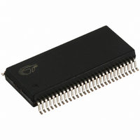
CY28RS480ZXC Cypress Semiconductor Corp, CY28RS480ZXC Datasheet - Page 9

CY28RS480ZXC
Manufacturer Part Number
CY28RS480ZXC
Description
IC CLOCK GENERATOR 56-TSSOP
Manufacturer
Cypress Semiconductor Corp
Type
Clock Generatorr
Datasheet
1.CY28RS480OXC.pdf
(15 pages)
Specifications of CY28RS480ZXC
Frequency - Max
200MHz
Voltage - Supply
3.135 V ~ 3.465 V
Operating Temperature
0°C ~ 70°C
Mounting Type
Surface Mount
Package / Case
56-TSSOP II
Frequency-max
200MHz
Lead Free Status / RoHS Status
Lead free / RoHS Compliant
Output
-
Input
-
Available stocks
Company
Part Number
Manufacturer
Quantity
Price
Company:
Part Number:
CY28RS480ZXC
Manufacturer:
MAXIM
Quantity:
160
Part Number:
CY28RS480ZXC
Manufacturer:
CYPRESS/赛普拉斯
Quantity:
20 000
Document #: 38-07638 Rev. *C
Absolute Maximum Conditions
DC Electrical Specifications
AC Electrical Specifications
V
V
V
T
T
T
ESD
Ø
Ø
UL-94
MSL
Multiple Supplies: The voltage on any input or I/O pin cannot exceed the power pin during power-up. Power supply sequencing is NOT required.
Crystal
T
T
Parameter
VDD_SRC1,
S
A
J
VDD_SRCS
DC
PERIOD
DD
DDA
IN
JC
JA
VDD_CPU,
VDD_SRC,
Parameter
Parameter
VDD_REF,
VDD_PCI,
V
V
VDD_48
IHSMBUS
ILSMBUS
HBM
C
IPD
IPD
V
V
V
V
C
V
I
I
V
L
I
OUT
OZ
DD
XIH
OH
XIL
IL
OL
IN
IH
IN
IL
D
T
Core Supply Voltage
Analog Supply Voltage
Input Voltage
Temperature, Storage
Temperature, Operating Ambient
Temperature, Junction
ESD Protection (Human Body Model)
Dissipation, Junction to Case
Dissipation, Junction to Ambient
Flammability Rating
Moisture Sensitivity Level
XIN Duty Cycle
XIN Period
3.3V Operating Voltage
Input Low Voltage
Input High Voltage
Input Low Voltage
Input High Voltage
Input Leakage Current
Output Low Voltage
Output High Voltage
High-Impedance Output Current
Input Pin Capacitance
Output Pin Capacitance
Pin Inductance
Xin High Voltage
Xin Low Voltage
Dynamic Supply Current
Power Down Supply Current
Power Down Supply Current
Description
Description
Description
3.3V ± 5%
SDATA, SCLK
SDATA, SCLK
VDD
Except pull-ups or pull-downs 0<V
I
I
At max load and frequency
PD asserted, Outputs driven
PD asserted, Outputs Hi-Z
OL
OH
= 1 mA
= 1 mA
The device will operate reliably with input
duty cycles up to 30/70 but the REF clock
duty cycle will not be within specification
When XIN is driven from an external
clock source
Relative to V
Non-functional
Functional
Functional
MIL-STD-883, Method 3015
Mil-Spec 883E Method 1012.1
JEDEC (JESD 51)
At 1/8 in.
Condition
Condition
SS
Condition
IN
<V
DD
V
0.7*V
69.841
2000
Min.
Min.
–0.5
–0.5
–0.5
3.135
47.5
SS
–65
Min.
–10
2.2
2.0
2.4
0
–
–
–
–5
–
–
3
3
–
0
–
–
–
–0.3
DD
CY28RS480
V–0
1
V
DD
Max.
+150
V
0.3*V
150
4.6
4.6
70
20
60
3.465
DD
–
Max.
Max.
52.5
71.0
+0.5
V
450
1.0
0.8
0.4
Page 9 of 15
10
75
12
5
–
5
5
7
DD
-
+0.3
DD
°C/W
°C/W
VDC
Unit
Unit
°C
°C
°C
Unit
V
V
V
mA
mA
mA
mA
µA
pF
pF
nH
ns
%
V
V
V
V
V
V
V
V
V
[+] Feedback


