CY28RS480ZXC Cypress Semiconductor Corp, CY28RS480ZXC Datasheet - Page 8
CY28RS480ZXC
Manufacturer Part Number
CY28RS480ZXC
Description
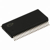
IC CLOCK GENERATOR 56-TSSOP
Manufacturer
Cypress Semiconductor Corp
Type
Clock Generatorr
Datasheet
1.CY28RS480OXC.pdf
(15 pages)
Specifications of CY28RS480ZXC
Frequency - Max
200MHz
Voltage - Supply
3.135 V ~ 3.465 V
Operating Temperature
0°C ~ 70°C
Mounting Type
Surface Mount
Package / Case
56-TSSOP II
Frequency-max
200MHz
Lead Free Status / RoHS Status
Lead free / RoHS Compliant
Output
-
Input
-
Available stocks
Company
Part Number
Manufacturer
Quantity
Price
Company:

Part Number:
CY28RS480ZXC
Manufacturer:
MAXIM
Quantity:
160
Part Number:
CY28RS480ZXC
Manufacturer:
CYPRESS/赛普拉斯
Quantity:
20 000


Document #: 38-07638 Rev. *C
CLK_REQ[0:1]# Description
The CLKREQ#[1:0] signals are active low input used for clean
stopping and starting selected SRC outputs. The outputs
controlled by CLKREQ#[1:0] are determined by the settings in
register bytes 4 and 5. The CLKREQ# signal is a debounced
signal in that its state must remain unchanged during two
consecutive rising edges of DIFC to be recognized as a valid
assertion or deassertion. (The assertion and deassertion of
this signal is absolutely asynchronous.)
CLK_REQ[0:1]# Deassertion [Low to High Transition]
The impact of deasserting the CLKREQ#[1:0] pins is all DIF
outputs that are set in the control registers to stoppable via
assertion of CLKREQ#[1:0] are to be stopped after their next
transition. When the control register CLKREQ# drive mode bit
is programmed to ‘0’, the final state of all stopped SRC signals
SRCC(free running)
SRCT(free running)
SRCT(stoppable)
SRCT(stoppable)
CLKREQ#X
Figure 3. CLK_REQ#[0:1] Assertion/Deassertion Waveform
is SRCT clock = High and SRCC = Low. There is to be no
change to the output drive current values, SRCT will be driven
high with a current value equal 6 x Iref,. When the control
register CLKREQ# drive mode bit is programmed to ‘1’, the
final state of all stopped DIF signals is low, both SRCT clock
and SRCC clock outputs will not be driven.
CLK_REQ[0:1]# Assertion [High to Low Transition]
All differential outputs that were stopped are to resume normal
operation in a glitch free manner. The maximum latency from
the Assertion to active outputs is between 2–6 SRC clock
periods (2 clocks are shown) with all SRC outputs resuming
simultaneously. If the CLKREQ# drive mode bit is
programmed to ‘1’ three-state), the all stopped SRC outputs
must be driven high within 10 ns of CLKREQ#[1:0] Assertion
to a voltage greater than 200 mV.
CY28RS480
Page 8 of 15
[+] Feedback
Related parts for CY28RS480ZXC
Image
Part Number
Description
Manufacturer
Datasheet
Request
R

Part Number:
Description:
Manufacturer:
Cypress Semiconductor Corp
Datasheet:
Part Number:
Description:
Manufacturer:
Cypress Semiconductor Corp
Datasheet:
Part Number:
Description:
Manufacturer:
Cypress Semiconductor Corp
Datasheet:
Part Number:
Description:
Manufacturer:
Cypress Semiconductor Corp
Datasheet:
Part Number:
Description:
Manufacturer:
Cypress Semiconductor Corp
Datasheet: