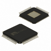
SY89534LHC Micrel Inc, SY89534LHC Datasheet - Page 9

SY89534LHC
Manufacturer Part Number
SY89534LHC
Description
IC SYNTHESIZR LVPECL/LVDS 64TQFP
Manufacturer
Micrel Inc
Series
Precision Edge®r
Type
Clock/Frequency Synthesizerr
Datasheet
1.SY89534LHZ.pdf
(15 pages)
Specifications of SY89534LHC
Pll
Yes with Bypass
Input
CMOS, HSTL, LVDS, LVPECL, LVTTL, SSTL
Output
LVPECL
Number Of Circuits
1
Ratio - Input:output
1:13
Differential - Input:output
Yes/Yes
Frequency - Max
500MHz
Divider/multiplier
Yes/No
Voltage - Supply
3 V ~ 3.6 V
Operating Temperature
0°C ~ 85°C
Mounting Type
Surface Mount
Package / Case
64-TQFP Exposed Pad, 64-eTQFP, 64-HTQFP, 64-VQFP
Frequency-max
500MHz
Lead Free Status / RoHS Status
Contains lead / RoHS non-compliant
Available stocks
Company
Part Number
Manufacturer
Quantity
Price
Micrel, Inc.
Output Logic Characteristics
illustrations. In cases where single-ended output is desired,
the designer should terminate the unused complimentary
output in the same manner as the normal output that is being
used. Unused LVPECL output pairs can be left floating.
Unused LVDS output pairs should be terminated
w/100 across the pair.
LVPECL operation:
LVDS operation (SY89535L, Bank B)
Thermal Considerations
dissipation. We strongly recommend soldering the exposed
die pad to a ground plane. Where this is not possible, we
recommend maintaining at least 500lfpm air flow around the
part.
M9999-110308
hbwhelp@micrel.com or (408) 955-1690
See “Output Termination Recommendations” for
• Typical voltage swing is 700mV
• Common mode voltage is V
• 100 termination across the output pair is NOT
• Typical voltage swing is 250mV
• Common mode voltage is 1.25V, typical.
• 100 termination across differential output pair is
This part has an exposed die pad for enhanced heat
50 .
recommended for LVPECL. See “Output Termination”
section, Figures 3 to 5.
effective 50 .
fine.
CC
–1.3V, typical.
PP
PP
to 800mV
to 450mV
PP
PP
into
into
9
REFCLK Input Interface
differential to single-ended input signal within 300mV above
V
true or complement inputs to ground, but not both. A logic zero
is achieved by connecting the complement input to ground
with the true input floating. For a TTL input, tie a 2.5k resistor
between the complement input and ground. See “Input
Interface” section, Figures 4a through 4j.
Input Levels
directly to the REFCLK inputs. Depending on the actual worst
case voltage seen, the minimum input voltage swing varies as
illustrated in the following table:
CC
The flexible REFCLK inputs are designed to accept any
Do not leave unused REFCLK inputs floating. Tie either the
LVDS, CML and HSTL differential signals may be connected
Input Voltage Range
and 300mV below ground.
0 to V
0 to 2.4V
/REFCLK
Figure 3. Simplified Input Structure
REFCLK
CC
+0.3
1.05k
1.05k
R1
R1
1.5k
R2
Minimum Voltage Swing
GND
V
CC
100mV
200mV
Precision Edge
R2
1.5k
SY89534/35L
®


