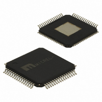
SY89534LHC Micrel Inc, SY89534LHC Datasheet - Page 6

SY89534LHC
Manufacturer Part Number
SY89534LHC
Description
IC SYNTHESIZR LVPECL/LVDS 64TQFP
Manufacturer
Micrel Inc
Series
Precision Edge®r
Type
Clock/Frequency Synthesizerr
Datasheet
1.SY89534LHZ.pdf
(15 pages)
Specifications of SY89534LHC
Pll
Yes with Bypass
Input
CMOS, HSTL, LVDS, LVPECL, LVTTL, SSTL
Output
LVPECL
Number Of Circuits
1
Ratio - Input:output
1:13
Differential - Input:output
Yes/Yes
Frequency - Max
500MHz
Divider/multiplier
Yes/No
Voltage - Supply
3 V ~ 3.6 V
Operating Temperature
0°C ~ 85°C
Mounting Type
Surface Mount
Package / Case
64-TQFP Exposed Pad, 64-eTQFP, 64-HTQFP, 64-VQFP
Frequency-max
500MHz
Lead Free Status / RoHS Status
Contains lead / RoHS non-compliant
Available stocks
Company
Part Number
Manufacturer
Quantity
Price
Micrel, Inc.
NOTES:
11. The within-device skew is defined as the worst case difference between any two similar delay paths within a single device operating at the same
12. The part-to-part skew is defined as the absolute worst case difference between any two delay paths on any two devices operating at the same
13. Cycle-to-cycle jitter definition: The variation in period between adjacent cycles over a random sample of adjacent cycle pairs. T
14. Period Jitter definition: For a specified amount of time (i.e., 1ms), there are N periods of a signal, and T
15. Using recommended loop filter components.
16. See “Timing Diagrams."
M9999-110308
hbwhelp@micrel.com or (408) 955-1690
All V
Symbol
f
f
t
t
t
t
t
t
t
t
t
t
t
FSEL-to-Valid Output Transition Time
IN
OUT
VCO
skew
LOCK
JITTER
pw
DC
r
OUTPUT_RESET
HOLD_FSEL
SETUP_FSEL
OUTPUT_SYNC
, t
AC ELECTRICAL CHARACTERISTICS
voltage and temperature.
voltage and temperature.
where T is the time between rising edges of the output signal.
signal. Period jitter is defined as the variation in the period of the output signal for corresponding edges relative to T
design and characterization.
f
(min)
CC
pins = +3.3V 10%
Reference Input Frequency
Output Frequency Range
Internal VCO Frequency Range
Within Device
Part-to-Part Skew
Maximum PLL Lock Time
Cycle-to-Cycle Jitter
Period Jitter
Minimum Pulse Width
Target PLL Loop Bandwidth
f
Output Rise/Fall Time
(20% to 80%)
(16)
OUT
(16)
Feedback Divider Ratio: 66
Feedback Divider Ratio: 30
(16)
(16)
Duty Cycle
(SY89535L) LVDS_Out
Parameter
(14)
(11)
(12)
Bank-to-Bank
LVPECL_Out
(13)
Within Bank
(Pk-to-Pk)
(rms)
(15)
(15)
Min.
600
—
—
—
—
—
—
—
—
—
—
—
—
—
—
—
—
—
—
—
T
A
Typ.
= 0 C
1.0
2.0
25
60
—
—
—
—
—
—
—
—
—
—
—
—
—
—
—
—
Max.
1000
6
150
400
450
50
50
—
—
—
—
—
—
—
—
—
—
—
—
—
—
33.33
Min.
600
14
50
45
—
—
—
—
—
—
—
—
—
—
—
—
5
5
1
T
A
= +25 C
Typ.
250
300
1.0
2.0
60
50
50
—
—
—
—
—
—
—
—
—
—
—
—
0
Max.
1000
n
160
500
200
400
450
150
50
10
50
50
—
—
—
55
10
—
—
—
—
is defined as the average period of that
Min.
600
50
45
—
—
—
—
—
—
—
—
—
—
—
—
—
—
—
—
—
n
. Parameter guaranteed by
T
A
= +85 C
Typ.
1.0
2.0
60
50
—
—
—
—
—
—
—
—
—
—
—
—
—
—
—
0
JITTER_CC
Precision Edge
Max.
1000
150
200
400
450
SY89534/35L
50
10
50
55
—
—
—
—
—
—
—
—
—
—
—
=T
n
–T
clock cycle
VCO
Unit
MHz
MHz
MHz
MHz
MHz
n+1
ms
ps
ps
ps
ps
ps
ns
ps
ns
ns
ns
ns
%
®


