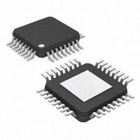
MAX9451EHJ+ Maxim Integrated Products, MAX9451EHJ+ Datasheet - Page 7

MAX9451EHJ+
Manufacturer Part Number
MAX9451EHJ+
Description
IC CLOCK GEN W/VCXO 32-TQFP
Manufacturer
Maxim Integrated Products
Type
Clock Generatorr
Datasheet
1.MAX9451EHJ.pdf
(18 pages)
Specifications of MAX9451EHJ+
Pll
Yes
Input
LVCMOS, LVDS, LVPECL
Output
HSTL
Number Of Circuits
1
Ratio - Input:output
2:2
Differential - Input:output
Yes/Yes
Frequency - Max
160MHz
Divider/multiplier
Yes/No
Voltage - Supply
2.4 V ~ 3.6 V
Operating Temperature
-40°C ~ 85°C
Mounting Type
Surface Mount
Package / Case
32-TQFP Exposed Pad, 32-eTQFP, 32-HTQFP, 32-VQFP
Frequency-max
160MHz
Lead Free Status / RoHS Status
Lead free / RoHS Compliant
The MAX9450/MAX9451/MAX9452 clock generators
provide high-precision clocks for timing in SONET/SDH
systems or Gigabit Ethernet systems. The MAX9450/
MAX9451/MAX9452 can also provide clocks for the
high-speed and high-resolution ADCs and DACs in 3G
base stations. Additionally, the MAX9450/MAX9451/
MAX9452 can be used as a jitter attenuator for generat-
ing high-precision clock signals.
The MAX9450/MAX9451/MAX9452 feature two differen-
tial inputs and two differential clock outputs. The inputs
accept LVPECL, LVDS, and LVCMOS signals. The
GND/CS
CMON
LOCK
SEL0
SEL1
IN0+
IN1+
IN0-
IN1-
SDA
SCL
AD0
AD1
INT
_______________________________________________________________________________________
MONITOR
Detailed Description
CLK
I
SPI PORT
2
C PORT
0
1
RJ
LUT FOR P
1/P
High-Precision Clock Generators
12kΩ TO 200kΩ
LOCK DET
PFD/CP
REGISTERS
CONTROL
60nF
LP2
LOOP FILTER
6nF
LUT FOR M
10kΩ
MR
input reference clock ranges from 8kHz to 500MHz and
the output clock ranges from 15MHz to 160MHz. The
internal clock monitor observes the condition of the
input reference clocks and provides a hitless switch
when an input failure is detected. The MAX9450/
MAX9451/MAX9452 also provide holdover in case no
input clock is supplied.
The MAX9450/MAX9451/MAX9452 contain eight 8-bit
control registers named CR0 to CR7. The registers are
accessible through the I
frequency-dividing factor, P. CR1 and CR2 hold the
values of the divider, M. CR3 and CR4 are for dividers
1/M
with Integrated VCXO
LP1
V
DDA
FUNDAMENTAL MODE
X1
15MHz TO 160MHz
AND AT CUT
GNDA
CRYSTAL
VCXO
Control and Status Registers
X2
V
DD
Functional Diagram
2
C/SPI interface. CR0 is for the
LUT FOR N1, N2
1/N0
DIV1
1/N1
DIV0
GND
MAX9450
MAX9451
MAX9452
MUX
CLK0+
CLK0-
CLK1+
CLK1-
OE
7


