AD9552BCPZ Analog Devices Inc, AD9552BCPZ Datasheet - Page 4
AD9552BCPZ
Manufacturer Part Number
AD9552BCPZ
Description
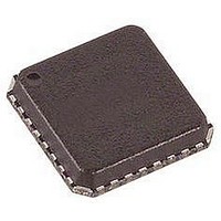
IC PLL CLOCK GEN LP 32LFCSP
Manufacturer
Analog Devices Inc
Type
Clock Generatorr
Datasheet
1.AD9552BCPZ-REEL7.pdf
(32 pages)
Specifications of AD9552BCPZ
Design Resources
Clock Distribution Circuit with Pin-Programmable Output Frequency, Output Logic Levels, and Fanout (CN0152)
Pll
Yes
Input
Clock, Crystal
Output
CMOS, LVDS, LVPECL
Number Of Circuits
1
Ratio - Input:output
2:2
Differential - Input:output
No/Yes
Frequency - Max
900MHz
Divider/multiplier
Yes/No
Voltage - Supply
3.3V
Operating Temperature
-40°C ~ 85°C
Mounting Type
Surface Mount
Package / Case
32-LFCSP
Frequency-max
900MHz
Clock Ic Type
Clock Generator
Ic Interface Type
Serial, SPI
Frequency
112.5MHz
No. Of Outputs
2
Supply Current
149mA
Digital Ic Case Style
LFCSP
No. Of Pins
32
Supply Voltage Range
3.135V To 3.465V
Rohs Compliant
Yes
Lead Free Status / RoHS Status
Lead free / RoHS Compliant
Available stocks
Company
Part Number
Manufacturer
Quantity
Price

Part Number:
AD9552BCPZ
Manufacturer:
ADI/亚德诺
Quantity:
20 000


AD9552
Parameter
VCO CHARACTERISTICS
1
2
3
4
5
6
7
CRYSTAL INPUT CHARACTERISTICS
Table 2.
Parameter
CRYSTAL FREQUENCY
CRYSTAL MOTIONAL RESISTANCE
CRYSTAL LOAD CAPACITANCE
OUTPUT CHARACTERISTICS
Table 3.
Parameter
LVPECL MODE
The A[2:0], Y[5:0], and OUTSEL pins have 100 kΩ internal pull-up resistors.
The RESET pin has a 100 kΩ internal pull-up resistor, so the default state of the device is reset.
N is the integer part of the feedback divider.
Sigma-delta modulator.
The minimum allowable feedback divider value with the SDM disabled.
The minimum allowable feedback divider value with the SDM enabled.
The frequency at the input to the phase-frequency detector.
Input Capacitance
Input Resistance
Duty Cycle
Input Voltage
Input High Voltage, V
Input Low Voltage, V
Input Threshold Voltage
Frequency Range
VCO Gain
VCO Tracking Range
VCO Calibration Time
Range
Tolerance
Differential Output Voltage Swing
Common-Mode Output Voltage
Frequency Range
Duty Cycle
Rise/Fall Time
Upper Bound
Lower Bound
1
(20% to 80%)
IH
IL
Min
40
0.52
±300
Min
10
Typ
3
130
4050
3350
45
140
1.0
Min
690
VDD − 1.77
0
40
Typ
26
15
Max
1.62
60
Max
52
20
100
Typ
765
VDD − 1.66
255
Unit
pF
kΩ
%
V
V
V
MHz
MHz
MHz/V
ppm
μs
Rev. C | Page 4 of 32
Test Conditions/Comments
When ac coupling to the input receiver, the user must dc bias the input
to 1 V
f
command (the rising edge of CS (Pin 12)) to the rising edge of LOCKED
(Pin 20).
Unit
MHz
ppm
Ω
pF
PFD
Max
889
VDD − 1.20
900
60
305
7
= 77.76 MHz; time between completion of the VCO calibration
Test Conditions/Comments
Using a crystal with a specified load capacitance other than
15 pF (8 pF to 24 pF) is possible, but necessitates using the
SPI port to configure the AD9552 crystal input capacitance.
Unit
mV
V
MHz
%
ps
Test Conditions/Comments
Output driver static
Output driver static
Up to 805 MHz output frequency
100 Ω termination between both pins of
the output driver
Related parts for AD9552BCPZ
Image
Part Number
Description
Manufacturer
Datasheet
Request
R

Part Number:
Description:
Oscillator Frequency Upconverter Eval Board
Manufacturer:
Analog Devices Inc
Datasheet:


Part Number:
Description:
±1.7g Dual-Axis IMEMS Accelerometer Evaluation Board
Manufacturer:
Analog Devices Inc
Datasheet:
Part Number:
Description:
Inertial Sensor Evaluation System
Manufacturer:
Analog Devices Inc
Datasheet:
Part Number:
Description:
Manufacturer:
Analog Devices Inc
Datasheet:
Part Number:
Description:
Manufacturer:
Analog Devices Inc
Datasheet:
Part Number:
Description:
Manufacturer:
Analog Devices Inc
Datasheet:
Part Number:
Description:
Manufacturer:
Analog Devices Inc
Datasheet:
Part Number:
Description:
Manufacturer:
Analog Devices Inc
Datasheet:
Part Number:
Description:
Manufacturer:
Analog Devices Inc
Datasheet:
Part Number:
Description:
Manufacturer:
Analog Devices Inc
Datasheet:
Part Number:
Description:
Manufacturer:
Analog Devices Inc
Datasheet:
Part Number:
Description:
Manufacturer:
Analog Devices Inc
Datasheet: