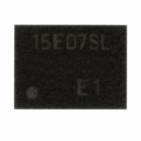
MB15E07SLPV1-G-6E1 Fujitsu Semiconductor America Inc, MB15E07SLPV1-G-6E1 Datasheet - Page 21

MB15E07SLPV1-G-6E1
Manufacturer Part Number
MB15E07SLPV1-G-6E1
Description
SYNTHESIZER PLL 2.5GHZ 16BCC
Manufacturer
Fujitsu Semiconductor America Inc
Type
Clock/Frequency Synthesizer, Prescalerr
Specifications of MB15E07SLPV1-G-6E1
Pll
Yes
Input
Clock
Output
Clock
Number Of Circuits
1
Ratio - Input:output
1:1
Differential - Input:output
Yes/No
Frequency - Max
2.5GHz
Divider/multiplier
Yes/No
Voltage - Supply
2.4 V ~ 3.6 V
Operating Temperature
-40°C ~ 85°C
Mounting Type
Surface Mount
Package / Case
16-LCC
Frequency-max
2.5GHz
Lead Free Status / RoHS Status
Lead free / RoHS Compliant
Other names
865-1002-2
Available stocks
Company
Part Number
Manufacturer
Quantity
Price
Company:
Part Number:
MB15E07SLPV1-G-6E1
Manufacturer:
Fujitsu Semiconductor America
Quantity:
135
Table 1. Control Bits
Single PLL Frequency Synthesizers with On-Chip Prescalers
Functional Descriptions
The VCO output frequency can be calculated using the following
equation:
f
f
M
N
A
f
R
20
Shift Register Configuration
VCO
VCO
OSC
Control Bit (CNT)
= {(M x N) + A} x f
Fujitsu Microelectronics, Inc.
Output frequency of external voltage controlled ocillator (VCO)
Preset divide ratio of dual modulus prescaler (64 or 128 for
Preset divide ratio of binary 11-bit programmable counter
Preset divide ratio of binary 7-bit swallow counter (0 A 127)
Reference oscillation frequency
Preset divide ratio of binary 14-bit programmable reference
MB15E03SL, MB15E05SL) (32 or 64 for MB15E07SL)
(3 to 2,047)
counter (3 to 16,383)
CNT
R1 to R14
SW
FC
LDS
CS
Note: Input data with MSB first.
H
L
Control bit
Divide ratio setting bits for the programmable reference counter (3 to 16,383)
Divide ratio setting bit for the prescaler
Phase control bit for the phase comparator
LD/f
Charge pump current select bit
OSC
OUT
Programmable reference counter latch
Programmable counter latch
signal select bit
R (A < N)
Destination of Serial Data
Serial Data Input
Serial data is entered using the Data, Clock and LE pins. The serial
data controls the programmable reference counters and the
programmable counters separately.
Binary serial data is entered through the Data pin when the LE pin
is held low. One bit of data is shifted into the shift register on the
rising edge of the Clock. When the LE signal pin is taken high,
entered data is latched into the appropriate counters according to
the control bit settings as follows:
[Table 1]
[Table 2]
[Table 5]
[Table 6]
[Table 7]
[Table 8]


