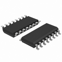
74HCT9046AD,118 NXP Semiconductors, 74HCT9046AD,118 Datasheet - Page 9

74HCT9046AD,118
Manufacturer Part Number
74HCT9046AD,118
Description
IC PLL BAND GAP CNTRL VCO 16SOIC
Manufacturer
NXP Semiconductors
Type
Phase Lock Loop (PLL)r
Series
74HCTr
Datasheet
1.74HCT9046AD118.pdf
(43 pages)
Specifications of 74HCT9046AD,118
Number Of Circuits
1
Package / Case
16-SOIC (3.9mm Width)
Pll
Yes
Input
Clock
Output
Clock
Ratio - Input:output
2:2
Differential - Input:output
No/No
Frequency - Max
16MHz
Divider/multiplier
No/No
Voltage - Supply
4.5 V ~ 5.5 V
Operating Temperature
-40°C ~ 125°C
Mounting Type
Surface Mount
Frequency-max
16MHz
Supply Voltage (max)
5.5 V
Supply Voltage (min)
4.5 V
Maximum Operating Temperature
+ 125 C
Minimum Operating Temperature
- 40 C
Mounting Style
SMD/SMT
Operating Supply Voltage
4.5 V to 5.5 V
Lead Free Status / RoHS Status
Lead free / RoHS Compliant
Lead Free Status / RoHS Status
Lead free / RoHS Compliant, Lead free / RoHS Compliant
Other names
568-1570-2
74HCT9046AD-T
935044180118
74HCT9046AD-T
935044180118
NXP Semiconductors
74HCT9046A_6
Product data sheet
8.3.2 Phase Comparator 2 (PC2)
This is a positive edge-triggered phase and frequency detector. When the PLL is using
this comparator, the loop is controlled by positive signal transitions and the duty cycles of
SIG_IN and COMP_IN are not important. PC2 comprises two D-type flip-flops, control
gating and a 3-state output stage with sink and source transistors acting as current
sources, henceforth called charge pump output of PC2. The circuit functions as an
up-down counter (see
count. The current switch charge pump output allows a virtually ideal performance of PC2,
due to appliance of some pulse overlap of the up and down signals, see
The pump current I
band gap reference of 2.5 V.
Where R
The current and voltage transfer function of PC2 are shown in
The phase comparator gain is:
I
K
cp
Fig 7.
P
=
=
17
--------- - A r
I
2
cp
bias
Typical waveforms for PLL using phase comparator 1; loop-locked at f
----------- - A
R
2.5
bias
is the external bias resistor between pin RB and ground.
cp
Rev. 06 — 15 September 2009
VCO_OUT
PC1_OUT
is independent from the supply voltage and is set by the internal
COMP_IN
VCO_IN
Figure
SIGN_IN
V
V
C1A
C1B
4) where SIG_IN causes an up-count and COMP_IN a down
PLL with band gap controlled VCO
74HCT9046A
Figure
mbd100
GND
V
C1A
C1B
CC
9.
© NXP B.V. 2009. All rights reserved.
Figure
0
8a.
9 of 43


