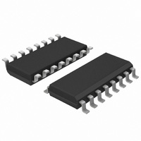
74HCT9046AD,118 NXP Semiconductors, 74HCT9046AD,118 Datasheet - Page 14

74HCT9046AD,118
Manufacturer Part Number
74HCT9046AD,118
Description
IC PLL BAND GAP CNTRL VCO 16SOIC
Manufacturer
NXP Semiconductors
Type
Phase Lock Loop (PLL)r
Series
74HCTr
Datasheet
1.74HCT9046AD118.pdf
(43 pages)
Specifications of 74HCT9046AD,118
Number Of Circuits
1
Package / Case
16-SOIC (3.9mm Width)
Pll
Yes
Input
Clock
Output
Clock
Ratio - Input:output
2:2
Differential - Input:output
No/No
Frequency - Max
16MHz
Divider/multiplier
No/No
Voltage - Supply
4.5 V ~ 5.5 V
Operating Temperature
-40°C ~ 125°C
Mounting Type
Surface Mount
Frequency-max
16MHz
Supply Voltage (max)
5.5 V
Supply Voltage (min)
4.5 V
Maximum Operating Temperature
+ 125 C
Minimum Operating Temperature
- 40 C
Mounting Style
SMD/SMT
Operating Supply Voltage
4.5 V to 5.5 V
Lead Free Status / RoHS Status
Lead free / RoHS Compliant
Lead Free Status / RoHS Status
Lead free / RoHS Compliant, Lead free / RoHS Compliant
Other names
568-1570-2
74HCT9046AD-T
935044180118
74HCT9046AD-T
935044180118
NXP Semiconductors
9. Limiting values
Table 3.
In accordance with the Absolute Maximum Rating System (IEC 60134). Voltages are referenced to GND (ground = 0 V).
[1]
[2]
74HCT9046A_6
Product data sheet
Symbol
V
I
I
I
I
I
T
P
IK
OK
O
CC
GND
Fig 13. Simple loop filter for PC2 with damping
CC
stg
tot
R bias
I
17
For DIP16 packages: above 70 C the value of P
For SO16 and TSSOP16 packages: above 70 C the value of P
cp
a. Simple loop filter for PC2 with
damping
1
2
Limiting values
=
=
Parameter
supply voltage
input clamping current
output clamping current
output current
supply current
ground current
storage temperature
total power dissipation
INPUT
R4 C2
R
----------- -
DIP16
SO16 and TSSOP16
17
bias
C2
R4
C2
I
cp
=
001aak446
OUTPUT
R3‘ C2
F
(j )
1/ A
Conditions
V
V
T
tot
A
m
Rev. 06 — 15 September 2009
b. Amplitude characteristic
0.5 V < V
amb
I
O
derates linearly with 12 mW/K.
< 0.5 V or V
< 0.5 V or V
1
F
= 40 C to +125 C
j
O
=
< V
tot
---------------------------- -
1 A
derates linearly with 8 mW/K.
1
1 /
I
CC
O
> V
+
A
> V
+
+ 0.5 V
2
j
CC
j
CC
2
+ 0.5 V
001aak447
+ 0.5 V
1
PLL with band gap controlled VCO
c. Pole zero diagram
[1]
[2]
A = DC gain limit, due to leakage
74HCT9046A
1/
Min
-
-
-
-
-
-
O
2
0.5
50
65
© NXP B.V. 2009. All rights reserved.
Max
+7
+50
-
+150
750
500
20
20
25
001aak448
1/ A
1
Unit
V
mA
mA
mA
mA
mA
mW
mW
C
14 of 43


