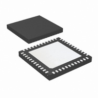
LMK03200ISQE/NOPB National Semiconductor, LMK03200ISQE/NOPB Datasheet - Page 24

LMK03200ISQE/NOPB
Manufacturer Part Number
LMK03200ISQE/NOPB
Description
IC CLOCK CONDITIONER PREC 48-LLP
Manufacturer
National Semiconductor
Type
Clock Conditionerr
Datasheet
1.LMK03200ISQENOPB.pdf
(40 pages)
Specifications of LMK03200ISQE/NOPB
Pll
Yes
Input
Clock
Output
LVDS, LVPECL
Number Of Circuits
1
Ratio - Input:output
1:9
Differential - Input:output
Yes/Yes
Frequency - Max
1.296GHz
Divider/multiplier
Yes/No
Voltage - Supply
3.15 V ~ 3.45 V
Operating Temperature
-40°C ~ 85°C
Mounting Type
Surface Mount
Package / Case
48-LLP
Frequency-max
1.296GHz
Lead Free Status / RoHS Status
Lead free / RoHS Compliant
Other names
LMK03200ISQETR
Available stocks
Company
Part Number
Manufacturer
Quantity
Price
Company:
Part Number:
LMK03200ISQE/NOPB
Manufacturer:
NSC
Quantity:
72
www.national.com
2.4 Register R0 to R7
Registers R0 through R7 control the eight clock outputs. Reg-
ister R0 controls CLKout0, Register R1 controls CLKout1, and
so on. There are some additional bit in register R0 called RE-
SET, DLD_MODE2, 0_DELAY_MODE, and FB_MUX. Aside
2.4.1 Reset bit -- Reset device to power on defaults
This bit is only in register R0. The use of this bit is optional
and it should be set to '0' if not used. Setting this bit to a '1'
forces all registers to their power on reset condition and there-
fore automatically clears this bit. If this bit is set, all other R0
bits are ignored and R0 needs to be programmed again if
used with its proper values and RESET = 0.
Bit Name
RESET
DLD_MODE2
0_DELAY_MODE
FB_MUX
CLKoutX_MUX
CLKoutX_EN
CLKoutX_DIV
CLKoutX_DLY
VCO_MUX
Vboost
DIV4
OSCin_FREQ
VCO_R4_LF
VCO_R3_LF
VCO_C3_C4_LF
EN_Fout
EN_CLKout_Global
POWERDOWN
PLL_MUX
PLL_R
PLL_R_DLY
PLL_CP_GAIN
VCO_DIV
PLL_N
PLL_N_DLY
Bit Value
Default
760
10
10
0
0
0
0
0
0
1
0
0
0
0
0
0
0
0
1
0
0
0
0
2
0
No reset, normal operation
Disabled
Disabled
CLKout5
Bypassed
Disabled
Divide by 2
0 ps
Use VCO divider
Normal Mode
PDF
10 MHz OSCin
Low (~200 Ω)
Low (~600 Ω)
C3 = 0 pF, C4 = 10 pF
Fout disabled
Normal - CLKouts normal
Normal - Device active
Disabled
R divider = 10
0 ps
100 µA
Divide by 2
N divider = 760
0 ps
Default Register Settings after Power on Reset
≤
20 MHz
Bit State
24
Reset to power on defaults
Digital Lock Detect Mode2 is disabled
Not 0-delay mode
0-delay mode feedback
CLKoutX mux mode
CLKoutX enable
CLKoutX clock divide
CLKoutX clock delay
VCO divider bypassed mode
Output Power Control
Phase Detector Frequency
OSCin Frequency in MHz
R4 internal loop filter values
R3 internal loop filter values
C3 and C4 internal loop filter values
Fout enable
Global clock output enable
Device power down
Multiplexer control for LD pin
PLL R divide value
PLL R delay value (lag)
Charge pump current
VCO divide value
PLL N divide value
PLL N delay value (lead)
from these, the functions of these bits in registers R0 through
R7 are identical. The X in CLKoutX_MUX, CLKoutX_DIV,
CLKoutX_DLY, and CLKoutX_EN denote the actual clock
output which may be from 0 to 7.
2.4.2 DLD_MODE2 bit -- Digital Lock Detect Mode 2
This bit is only in register R0. The output of the LD pin is de-
fined by register PLL_MUX (See
tiplexer Control for LD
is selected, setting this bit overrides the default functionality
allowing the user to determine when the frequency calibration
routine is done. When using 0-delay mode this informs the
user when the 0-delay mode can be activated. See section
2.2 Recommended Programing Sequence, with 0-Delay
Mode
DLD_MODE2
0 (default)
for more information.
1
1
Bit Description
0_DELAY_MODE
Pin). When a Digital Lock Detect output
X
0
1
2.9.2 PLL_MUX[3:0] -- Mul-
Register
R0 to R7
Digital Lock Detect
Digital Lock Detect
Digital Calibration
R11
R13
R14
R15
R0
R7
R9
LD Output
Complete
Location
26:25
18:17
26:25
21:14
13:11
23:20
31:30
29:26
15:8
10:8
19:8
25:8
7:4
7:4
7:4
7:4
Bit
31
28
27
16
16
15
28
27
26


