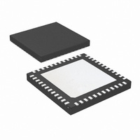
LMK03200ISQE/NOPB National Semiconductor, LMK03200ISQE/NOPB Datasheet - Page 19

LMK03200ISQE/NOPB
Manufacturer Part Number
LMK03200ISQE/NOPB
Description
IC CLOCK CONDITIONER PREC 48-LLP
Manufacturer
National Semiconductor
Type
Clock Conditionerr
Datasheet
1.LMK03200ISQENOPB.pdf
(40 pages)
Specifications of LMK03200ISQE/NOPB
Pll
Yes
Input
Clock
Output
LVDS, LVPECL
Number Of Circuits
1
Ratio - Input:output
1:9
Differential - Input:output
Yes/Yes
Frequency - Max
1.296GHz
Divider/multiplier
Yes/No
Voltage - Supply
3.15 V ~ 3.45 V
Operating Temperature
-40°C ~ 85°C
Mounting Type
Surface Mount
Package / Case
48-LLP
Frequency-max
1.296GHz
Lead Free Status / RoHS Status
Lead free / RoHS Compliant
Other names
LMK03200ISQETR
Available stocks
Company
Part Number
Manufacturer
Quantity
Price
Company:
Part Number:
LMK03200ISQE/NOPB
Manufacturer:
NSC
Quantity:
72
serted active high or low depending on PLL_MUX value to
indicate the device is phase locked. 0_DELAY_MODE = 1
reverts the LD pin back to digital lock detect.
The device is now phase locked and synchronized with the
reference clock. Since step 2 requires GOE high for feedback,
it is possible that the clock outputs will be momentarily slightly
off frequency while the dividers and or feedback paths are
being changed. Also when GOE is set high, it is possible for
a runt pulse to occur since GOE is an asynchronous input. If
there is no concern for off frequency clock cycles then it is
allowable to leave GOE high for the entire programming pro-
cedure.
Before 0-delay mode the VCO frequency equation is: VCO
Frequency = Reference OSCin Frequency / PLL R Divider *
PLL N Divider * VCO divider.
After 0-delay mode the VCO frequency equation is: VCO Fre-
quency = Reference OSCin Frequency / PLL R Divider * PLL
N
CLKoutX_DIV is the divide value of the clock used for feed-
back. If the clock is from FBCLKin, any external divides must
also be accounted for.
2.2.1 0-Delay Mode Example 1
In this example assume the user requirements are: an input
reference of 10 MHz and a clock output of 30 MHz with the
clock output synchronized to the reference input clock. CLK-
out5 is chosen as the output clock because it allows internal
feedback for the 0-delay mode.
Registers which are not explicitly programmed are set to de-
fault values.
Step 1
•
•
•
•
•
•
•
•
•
The device now begins the frequency calibration routine,
when it completes the LD pin will go high since PLL_MUX was
programmed with the active high option for the frequency cal-
ibration routine complete signal. When the LD pin goes high,
step 2 is executed.
GOE pin is set low.
Program Register 0 (reset device)
RESET = 1
Other values don't matter
Program Register 0 again.
RESET = 0
DLD_MODE2 = 1 (Digital Lock detect will be used for
monitoring frequency calibration routine complete)
FB_MUX = 0 (CLKout5 feedback)
Program Register 5 (30 MHz, used for feedback)
CLKout5_EN = 1 (turn output on)
CLKout5_MUX = 1 (divided)
CLKout5_DIV = 10 (divide by 20)
Program Register 6 (Must be enabled when using
CLKout5 for feedback)
CLKout6_EN = 1 (turn output on)
Program Register 8
Program Register 14
PLL_R = 1 (Phase detector frequency = 10 MHz)
PLL_MUX = 3 (DLD Active High)
Program Register 15 (VCO Frequency = 1200 MHz)
PLL_N = 60
VCO_DIV = 2
PLL_CP_GAIN = Loop filter dependant
Begin monitoring LD pin for frequency calibration routine
complete signal.
Divider
*
VCO
divider
*
CLKoutX_DIV.
Where
19
Step 2
•
•
•
The device will now synchronize. As soon as the device is
settled the LD pin will go high to indicate the device is phase
locked (0_DELAY_MODE = 1 reverts the LD pin back to dig-
ital lock detect mode). Now the device's VCO will be locked
to 1200 MHz with an output clock of 30 MHz.
2.2.2 0-Delay Mode Example 2
In this example assume the user requirements are: an input
reference of 61.44 MHz and clock outputs of 12.288 MHz
(CLKout6), 30.72 MHz (CLKout3), and 61.44 MHz (CLKout4)
with the clock outputs synchronized to the reference input
clock. CLKout6 is chosen for feedback since the 12.288 MHz
clock is the lowest frequency required to be synchronized (0-
delay) with the reference and therefore must be fed back to
the PLL N divider, note this also limits the phase detector fre-
quency to 12.288 MHz so the input reference must be divided
down to 12.288 MHz. If the 12.288 MHz clock wasn't required
to be in synchronization (0-delay) with the reference, the
30.72 MHz clock could have been fed back instead rasing the
maximum allowable phase detector frequency to 30.72 MHz.
Registers which are not explicitly programmed are set to de-
fault values.
Step 1
•
•
•
•
•
•
•
•
•
Set GOE pin high.
Program Register 0
RESET = 0
0_DELAY_MODE = 1 (activate 0-delay mode)
DLD_MODE2 = 1 (same, don't care)
FB_MUX = 0 (same)
Program Register 15 (VCO Frequency = 1200 MHz)
PLL_N = 3 (updated value)
VCO_DIV = 2 (same)
PLL_CP_GAIN = Loop filter dependant
GOE pin is set low.
Program Register 0 (reset device)
RESET = 1
Other values don't matter
Program Register 0 again.
RESET = 0
DLD_MODE2 = 1 (Digital Lock detect will be used for
monitoring frequency calibration routine complete)
FB_MUX = 2 (CLKout6 feedback)
Program Register 3 (30.72 MHz)
CLKout3_EN = 1 (turn output on)
CLKout3_MUX = 1 (divided)
CLKout3_DIV = 10 (divide by 20)
Program Register 4 (61.44 MHz)
CLKout4_EN = 1 (turn output on)
CLKout4_MUX = 1 (divided)
CLKout4_DIV = 5 (divide by 10)
Program Register 6 (12.288 MHz, used for feedback)
CLKout6_EN = 1 (turn output on)
CLKout6_MUX = 1 (divided)
CLKout6_DIV = 25 (divide by 50)
Program Register 8
Program Register 14
PLL_R = 5 (Phase detector frequency = 12.288 MHz)
PLL_MUX = 3 (DLD Active High)
Program Register 15 (VCO Frequency = 1228.8 MHz)
PLL_N = 50
VCO_DIV = 2
PLL_CP_GAIN = Loop filter dependant
www.national.com


