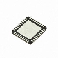
SI5317D-C-GM Silicon Laboratories Inc, SI5317D-C-GM Datasheet - Page 24

SI5317D-C-GM
Manufacturer Part Number
SI5317D-C-GM
Description
IC CLK JITTER CLEANR PROG 36QFN
Manufacturer
Silicon Laboratories Inc
Type
Jitter Cleanerr
Series
Si5317r
Datasheet
1.SI5317C-C-GM.pdf
(46 pages)
Specifications of SI5317D-C-GM
Package / Case
36-QFN
Pll
Yes with Bypass
Input
Clock, Crystal
Output
CML, CMOS, LVDS, LVPECL
Number Of Circuits
1
Ratio - Input:output
1:2
Differential - Input:output
Yes/Yes
Frequency - Max
100MHz
Divider/multiplier
No/No
Voltage - Supply
1.71 V ~ 3.63 V
Operating Temperature
-40°C ~ 85°C
Mounting Type
Surface Mount
Frequency-max
100MHz
Termination Style
SMD/SMT
Output Format
CML
Dimensions
5 mm W x 7 mm L x 1.85 mm H
Minimum Operating Temperature
- 40 C
Maximum Operating Temperature
+ 85 C
Mounting Style
SMD/SMT
Product
XO
Frequency
10 MHz to 945 MHz
Frequency Stability
+/- 20 PPM
Supply Voltage
3.3 Volts
Height
1.85 mm
Lead Free Status / RoHS Status
Lead free / RoHS Compliant
Lead Free Status / RoHS Status
Lead free / RoHS Compliant, Lead free / RoHS Compliant
Other names
336-1920
Si5317
3.6. PLL Bypass Mode
The Si5317 supports a PLL bypass mode in which the selected input clock is fed directly to both enabled output
buffers, bypassing the DSPLL. Internally, the bypass path is implemented with high-speed signaling; however, this
path is not a low jitter path and will result in significantly higher jitter on CKOUT. In PLL bypass mode, the input and
output clocks will be at the same frequency. PLL bypass mode is useful as a debug tool. The DSBL2_BY pin is
used to select the PLL Bypass Mode according to Table 11. Bypass mode is not supported for CMOS clock
outputs.
24
FRQSEL[3:0]
BWSEL[1:0]
FRQTBL
CKIN+
CKIN–
DEC
LOS
LOL
RST
INC
2
Skew Control
DSBL2/BYPASS
Bandwidth
Frequency
Control
Control
Control
Alarms
M
H
L
Table 11. DSBL2/BYPASS Pin Settings
f
RATE[1:0]
3
Figure 6. Bypass Signal
External Crystal or
XB
Reference Clock
PLL Bypass Mode w/ CKOUT2 Enabled
DSPLL
Rev. 1.1
®
CKOUT2 Disabled
CKOUT2 Enabled
XA
Function
PLL Bypass
f
OSC
Regulator with
High PSRR
Voltage
0
0
1
1
2
2
VDD (1.8, 2.5, or 3.3 V)
GND
CKOUT+
CKOUT–
DBL2_BY
CKOUT+
CKOUT–
SFOUT[1:0]


