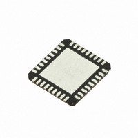
SI5317D-C-GM Silicon Laboratories Inc, SI5317D-C-GM Datasheet - Page 15

SI5317D-C-GM
Manufacturer Part Number
SI5317D-C-GM
Description
IC CLK JITTER CLEANR PROG 36QFN
Manufacturer
Silicon Laboratories Inc
Type
Jitter Cleanerr
Series
Si5317r
Datasheet
1.SI5317C-C-GM.pdf
(46 pages)
Specifications of SI5317D-C-GM
Package / Case
36-QFN
Pll
Yes with Bypass
Input
Clock, Crystal
Output
CML, CMOS, LVDS, LVPECL
Number Of Circuits
1
Ratio - Input:output
1:2
Differential - Input:output
Yes/Yes
Frequency - Max
100MHz
Divider/multiplier
No/No
Voltage - Supply
1.71 V ~ 3.63 V
Operating Temperature
-40°C ~ 85°C
Mounting Type
Surface Mount
Frequency-max
100MHz
Termination Style
SMD/SMT
Output Format
CML
Dimensions
5 mm W x 7 mm L x 1.85 mm H
Minimum Operating Temperature
- 40 C
Maximum Operating Temperature
+ 85 C
Mounting Style
SMD/SMT
Product
XO
Frequency
10 MHz to 945 MHz
Frequency Stability
+/- 20 PPM
Supply Voltage
3.3 Volts
Height
1.85 mm
Lead Free Status / RoHS Status
Lead free / RoHS Compliant
Lead Free Status / RoHS Status
Lead free / RoHS Compliant, Lead free / RoHS Compliant
Other names
336-1920
Si5317
3. Frequency Plan Tables
For ease of use, the Si5317 is pin-controlled to enable simple device configuration of the frequency range plan and
PLL loop bandwidth via a predefined look-up table. The DSPLL has been optimized for jitter performance and
tunability for each frequency range and PLL loop bandwidth provided in Table 9 on page 22.
Many of the control inputs are three levels: High, Low, and Medium. High and Low are standard voltage levels
determined by the supply pins: V
and Ground. If the input pin is left floating, it is driven to nominally half of V
.
DD
DD
Effectively, this creates three logic levels for these controls. See section 6. "Power Supply Filtering" on page 33 and
section 1.2. "Three-Level Input Pins (Example with External Resistors)" on page 9 for additional information.
3.1. Frequency Range Plan
The input to output clock frequency range is set by the 3-level FRQSEL[3:0] and FRQTBL pins. The CKIN and
CKOUT is the same frequency range as specified in Table 8. Due to the wide tunability of the Si5317, each
frequency plan provides overlap between adjacent settings. To select a frequency plan, the desired frequency
should be selected as close to the defined center frequency. In certain cases where the desired frequency is
exactly between two overlapping plans, either FRQTBL and FRQSEL setting can be used.
3.1.1. PLL Loop Bandwidth Plan
The Si5317's loop bandwidth ranges from 60 Hz to 8.4 kHz. For each frequency range, the corresponding loop
bandwidth is provided in a simple look-up table (see Table 9 on page 22). The loop bandwidth is digitally
programmable using the three-level BWSEL [1:0] input pins.
3.2. Output Skew Adjustment
The overall device skew (CKIN to CKOUTn phase delay) is adjustable via the INC and DEC input pins. A positive
edge triggered pulse applied to the INC pin increases the device skew defined by Table 8, INC/DEC step size, for
each given frequency plan. The identical operation on the DEC pin decreases the skew by the same amount.
Using the INC and DEC pins, there is no limit to the range of skew adjustment that can be made. Following a
powerup or reset, the overall device skew will revert to the reset value, although the input-to-output skew is
effectively random. The rate of change for each INC/DEC operation is defined by the selected loop bandwidth,
BWSEL[1:0].
Rev. 1.1
15


