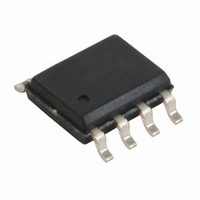
CY2305CSXC-1H Cypress Semiconductor Corp, CY2305CSXC-1H Datasheet - Page 8

CY2305CSXC-1H
Manufacturer Part Number
CY2305CSXC-1H
Description
IC CLK ZDB 5OUT 133MHZ 8SOIC
Manufacturer
Cypress Semiconductor Corp
Type
Fanout Distribution, Zero Delay Bufferr
Datasheet
1.CY2305CSXC-1H.pdf
(17 pages)
Specifications of CY2305CSXC-1H
Number Of Circuits
1
Package / Case
8-SOIC (3.9mm Width)
Pll
Yes
Input
LVCMOS, LVTTL
Output
LVCMOS
Ratio - Input:output
1:5
Differential - Input:output
No/No
Frequency - Max
133.33MHz
Divider/multiplier
No/No
Voltage - Supply
3 V ~ 3.6 V
Operating Temperature
0°C ~ 70°C
Mounting Type
Surface Mount
Frequency-max
133MHz
Output Frequency Range
10 MHz to 133.33 MHz
Supply Voltage (max)
3.6 V
Supply Voltage (min)
3 V
Maximum Operating Temperature
+ 70 C
Minimum Operating Temperature
0 C
Mounting Style
SMD/SMT
Operating Supply Voltage
3.3 V
Lead Free Status / RoHS Status
Lead free / RoHS Compliant
Lead Free Status / RoHS Status
Lead free / RoHS Compliant, Lead free / RoHS Compliant
Other names
428-2194-5
CY2305CSXC-1H
CY2305CSXC-1H
Available stocks
Company
Part Number
Manufacturer
Quantity
Price
Part Number:
CY2305CSXC-1H
Manufacturer:
CYPRESS/赛普拉斯
Quantity:
20 000
Company:
Part Number:
CY2305CSXC-1HT
Manufacturer:
ABC
Quantity:
84 000
Part Number:
CY2305CSXC-1HT
Manufacturer:
CYPRESS/赛普拉斯
Quantity:
20 000
Switching characteristics table for CY2305CSXC-1H and CY2309CSXC-1H commercial temperature devices. All parameters are
specified with loaded outputs.
Switching Characteristics for CY2305CSXI-XX, CY2305CSXA-XX and CY2309CSXI-XX
Switching characteristics table for CY2305CSXI-1, CY2305CSXA-1, and CY2309CSXI-1 industrial temperature devices. All
parameters are specified with loaded outputs.
Document Number: 38-07672 Rev. *K
Note
t
t
t
t
t
t
t
t
t
t
t
t
t
t
t
t
t
t
t
t
t
Switching Characteristics for CY2305CSXC-XX and CY2309CSXC-XX
1
DC
3
4
5
6A
6B
7
8
J
LOCK
1
DC
3
4
5
6A
6B
7
J
LOCK
11. Parameter is guaranteed by design and characterization. Not 100% tested in production.
Parameter
Parameter
Output frequency
Output duty cycle
Rise time
Fall time
Output-to-output skew
Delay, REF rising edge to
CLKOUT rising edge
Delay, REF rising edge to
CLKOUT rising edge
Device-to-device skew
Cycle-to-cycle jitter, peak
PLL lock time
Output frequency
Output duty cycle
Rise time
Fall time
Output-to-output skew
Delay, REF rising edge to
CLKOUT rising edge
Delay, REF rising edge to
CLKOUT rising edge
Device-to-device skew
Output slew rate
Cycle-to-cycle jitter, peak
PLL lock time
[11]
[11]
[11]
[11]
Name
Name
[11]
[11]
[11]
[11]
[11]
[11]
[11]
= t
= t
[11]
[11]
[11]
[11]
[11]
[11]
2
2
t
t
[11]
[11]
1
1
30-pF load
10-pF load
Measured at 1.4 V, F
Measured at 1.4 V, F
Measured between 0.8 V and 2.0 V
Measured between 0.8 V and 2.0 V
All outputs equally loaded
Measured at V
Measured at V
Bypass mode, CY2309C device only.
Measured at V
of devices
Measured between 0.8 V and 2.0 V using
Test circuit #2
Measured at 66.67 MHz, loaded outputs
Stable power supply, valid clock
presented on REF pin
30 pF load
10 pF load
Measured at 1.4 V, F
Measured at 1.4 V, F
Measured between 0.8 V and 2.0 V
Measured between 0.8 V and 2.0 V
All outputs equally loaded
Measured at V
Measured at V
Bypass mode, CY2309C device only.
Measured at V
of devices
Measured at 66.67 MHz, loaded outputs
Stable power supply, valid clock
presented on REF pin
Test Conditions
Description
DD
DD
DD
DD
DD
DD
/2
/2. Measured in PLL
/2 on the CLKOUT pins
/2 on the CLKOUT pins
/2
/2. Measured in PLL
out
out
out
out
> 50 MHz
50 MHz
> 50 MHz
<= 50 MHz
Min
10
10
40
45
Min
–
–
–
–
1
–
–
–
10
10
40
45
–
–
–
–
1
–
1
–
–
Typ
50
50
50
Typ
–
–
–
–
0
5
0
–
50
50
–
–
–
–
0
5
0
–
–
–
133.33
133.33
±350
Max
2.25
2.25
100
200
700
175
±350
8.7
1.0
Max
60
55
100
200
700
175
1.5
1.5
8.7
1.0
60
55
–
CY2305C
CY2309C
Page 8 of 17
MHz
MHz
Unit
MHz
MHz
V/ns
Unit
ms
ns
ns
ps
ps
ns
ps
ps
%
%
ms
ns
ns
ps
ps
ns
ps
ps
%
%
[+] Feedback


