NB7L14MNTXG ON Semiconductor, NB7L14MNTXG Datasheet - Page 2
NB7L14MNTXG
Manufacturer Part Number
NB7L14MNTXG
Description
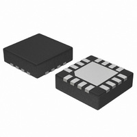
IC FANOUT BUFFER DIFF 16-QFN
Manufacturer
ON Semiconductor
Series
GigaComm™r
Type
Fanout Buffer (Distribution)r
Datasheet
1.NB7L14MNTXG.pdf
(9 pages)
Specifications of NB7L14MNTXG
Number Of Circuits
1
Ratio - Input:output
1:4
Differential - Input:output
Yes/Yes
Input
CML, LVCMOS, LVDS, LVPECL, LVTTL
Output
LVPECL
Frequency - Max
8GHz
Voltage - Supply
2.375 V ~ 3.6 V
Operating Temperature
-40°C ~ 85°C
Mounting Type
Surface Mount
Package / Case
16-TFQFN Exposed Pad
Frequency-max
8GHz
Lead Free Status / RoHS Status
Lead free / RoHS Compliant
Available stocks
Company
Part Number
Manufacturer
Quantity
Price
Company:

Part Number:
NB7L14MNTXG
Manufacturer:
ON Semiconductor
Quantity:
1 300
Part Number:
NB7L14MNTXG
Manufacturer:
ON/安森美
Quantity:
20 000


1. In the differential configuration when the input termination pin (VT) is connected to a common termination voltage or left open, and if no signal
2. All VCC and GND pins must be externally connected to a power supply for proper operation.
Table 1. PIN DESCRIPTION
Pin
10
12
13
14
15
16
11
1
2
3
4
5
6
7
8
9
−
is applied on IN/IN input, then, the device will be susceptible to self−oscillation.
VREFAC
Name
GND
GND
VCC
VCC
Q3
Q3
Q2
Q2
Q1
Q1
Q0
Q0
EP
VT
IN
IN
LVPECL Output
LVPECL Output
LVPECL Output
LVPECL Output
LVPECL Output
LVPECL Output
LVPECL Output
LVPECL Output
LVDS, LVTTL
LVDS, LVTTL
ECL, CML,
ECL, CML,
LVCMOS,
LVCMOS,
Input
Input
I/O
−
−
−
−
−
−
V
REFAC
Non−inverted Differential Input. Note 1. Internal 50 W Resistor to Termination Pin, VT
Internal 50−W Termination Pin for IN/IN inputs.
Output Reference Voltage for capacitor−coupled inputs
Inverted Differential Input. Note 1. Internal 50 W Resistor to Termination Pin, VT.
Negative Supply Voltage
Inverted Differential Output. Typically Terminated with 50 W Resistor to V
Non−inverted Differential Output. Typically Terminated with 50 W Resistor to V
Positive Supply Voltage
Inverted Differential Output. Typically Terminated with 50 W Resistor to V
Non−inverted Differential Output. Typically Terminated with 50 W Resistor to V
Inverted Differential Output. Typically Terminated with 50 W Resistor to V
Non−inverted Differential Output. Typically Terminated with 50 W Resistor to V
Positive Supply Voltage
Inverted Differential Output. Typically Terminated with 50 W Resistor to V
Non−inverted Differential Output. Typically Terminated with 50 W Resistor to V
Negative Supply Voltage
The Exposed Pad (EP) on the QFN−16 package bottom is thermally connected to the die for im-
proved heat transfer out of package. The exposed pad must be attached to a heat−sinking con-
duit. The pad is electrically connected to the die, and must be electrically connected to device
GND.
VT
IN
IN
Figure 2. QFN−16 Pinout (Top View)
1
2
3
4
GND Q0
GND
16
5
http://onsemi.com
15
Q3
NB7L14
6
Q0
14
Q3
2
7
V
V
13
8
CC
CC
Exposed Pad (EP)
Description
12
11
10
9
Q1
Q1
Q2
Q2
CC
CC
CC
CC
– 2.0 V.
– 2.0 V.
– 2.0 V.
– 2.0 V.
CC
CC
CC
CC
– 2.0 V.
– 2.0 V.
– 2.0 V.
– 2.0 V.
Related parts for NB7L14MNTXG
Image
Part Number
Description
Manufacturer
Datasheet
Request
R

Part Number:
Description:
2.5v/3.3vdifferential 1 4 Clock/data Fanout Buffer/translator With Cml Outputs And Internal Termination
Manufacturer:
ON Semiconductor
Datasheet:
Part Number:
Description:
2.5v / 3.3v 7ghz/10gbps Differential 1 4 Lvpecl Fanout Buffer
Manufacturer:
ON Semiconductor
Datasheet:
Part Number:
Description:
ON Semiconductor [VOLTAGE REGULATOR]
Manufacturer:
ON Semiconductor
Datasheet:
Part Number:
Description:
357-036-542-201 CARDEDGE 36POS DL .156 BLK LOPRO
Manufacturer:
ON Semiconductor
Datasheet:
Part Number:
Description:
357-036-542-201 CARDEDGE 36POS DL .156 BLK LOPRO
Manufacturer:
ON Semiconductor
Datasheet:
Part Number:
Description:
357-036-542-201 CARDEDGE 36POS DL .156 BLK LOPRO
Manufacturer:
ON Semiconductor
Datasheet:
Part Number:
Description:
357-036-542-201 CARDEDGE 36POS DL .156 BLK LOPRO
Manufacturer:
ON Semiconductor
Datasheet:
Part Number:
Description:
357-036-542-201 CARDEDGE 36POS DL .156 BLK LOPRO
Manufacturer:
ON Semiconductor
Datasheet:
Part Number:
Description:
357-036-542-201 CARDEDGE 36POS DL .156 BLK LOPRO
Manufacturer:
ON Semiconductor
Datasheet:
Part Number:
Description:
357-036-542-201 CARDEDGE 36POS DL .156 BLK LOPRO
Manufacturer:
ON Semiconductor
Datasheet:
Part Number:
Description:
357-036-542-201 CARDEDGE 36POS DL .156 BLK LOPRO
Manufacturer:
ON Semiconductor
Datasheet:
Part Number:
Description:
357-036-542-201 CARDEDGE 36POS DL .156 BLK LOPRO
Manufacturer:
ON Semiconductor
Datasheet:
Part Number:
Description:
357-036-542-201 CARDEDGE 36POS DL .156 BLK LOPRO
Manufacturer:
ON Semiconductor
Datasheet:
Part Number:
Description:
Manufacturer:
ON Semiconductor
Datasheet: