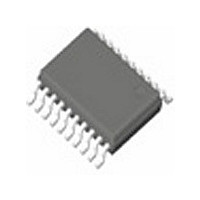
IDT8535-01PGG8 IDT, Integrated Device Technology Inc, IDT8535-01PGG8 Datasheet - Page 3

IDT8535-01PGG8
Manufacturer Part Number
IDT8535-01PGG8
Description
IC FANOUT BUFFER LVPECL 20-TSSOP
Manufacturer
IDT, Integrated Device Technology Inc
Type
Fanout Buffer (Distribution), Multiplexerr
Specifications of IDT8535-01PGG8
Number Of Circuits
1
Ratio - Input:output
2:4
Differential - Input:output
No/Yes
Input
LVCMOS, LVTTL
Output
LVPECL
Frequency - Max
266MHz
Voltage - Supply
3.135 V ~ 3.465 V
Operating Temperature
0°C ~ 70°C
Mounting Type
Surface Mount
Package / Case
20-TSSOP
Frequency-max
266MHz
Number Of Clock Inputs
2
Mode Of Operation
Single-Ended
Output Frequency
266MHz
Output Logic Level
LVPECL
Operating Supply Voltage (min)
3.135V
Operating Supply Voltage (typ)
3.3V
Operating Supply Voltage (max)
3.465V
Package Type
TSSOP
Operating Temp Range
0C to 70C
Operating Temperature Classification
Commercial
Signal Type
LVCMOS/LVTTL
Mounting
Surface Mount
Pin Count
20
Lead Free Status / RoHS Status
Lead free / RoHS Compliant
Other names
8535-01PGG8
CONTROL INPUT FUNCTION TABLE
NOTES:
1. After CLK_EN switches, the clock outputs are disabled or enabled following a rising and falling input clock edge as shown in the CLK_EN Timing Diagram below.
2. In active mode, the state of the outputs is a function of the CLK / xCLK and PCLK / xPCLK inputs as described in the Clock Input Function table.
CLOCK INPUT FUNCTION TABLE
NOTE:
1. H = HIGH
xQ0, xQ1, xQ2, xQ3
IDT8535-01
LOW SKEW, 1-TO-4 LVCMOS-TO-3.3V LVPECL
L = LOW
Q0, Q1, Q2, Q3
CLK0 or CLK1
CLK0, CLK1
CLK_EN
Inputs
0
0
1
1
CLK_EN
0
1
Q0 to Q3
CLK_SEL
H
Inputs
L
0
1
0
1
Outputs
Disabled
xQ0 to xQ3
H
L
CLK_EN Timing Diagram
Selected Source
(1)
CLK0
CLK1
CLK0
CLK1
(1,2)
3
≈
≈
≈
COMMERCIAL AND INDUSTRIAL TEMPERATURE RANGES
Disabled; LOW
Disabled; LOW
Q0 to Q3
Enabled
Enabled
Enabled
Outputs
Disabled; HIGH
Disabled; HIGH
xQ0 to xQ3
Enabled
Enabled


