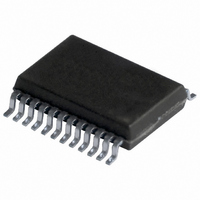
PCK351DB,112 NXP Semiconductors, PCK351DB,112 Datasheet - Page 6

PCK351DB,112
Manufacturer Part Number
PCK351DB,112
Description
IC CLOCK DISTRIB 1:10 24SSOP
Manufacturer
NXP Semiconductors
Type
Fanout Buffer (Distribution)r
Datasheet
1.PCK351D112.pdf
(18 pages)
Specifications of PCK351DB,112
Package / Case
24-SSOP
Mounting Type
Surface Mount
Voltage - Supply
3 V ~ 3.6 V
Frequency-max
125MHz
Operating Temperature
-40°C ~ 85°C
Output
LVTTL
Number Of Circuits
1
Input
LVTTL
Ratio - Input:output
1:10
Differential - Input:output
No/No
Number Of Outputs
10
Propagation Delay (max)
4.1 ns
Supply Voltage (max)
3.6 V
Supply Voltage (min)
3 V
Maximum Power Dissipation
1700 mW
Maximum Operating Temperature
+ 85 C
Minimum Operating Temperature
- 40 C
Mounting Style
SMD/SMT
Lead Free Status / RoHS Status
Lead free / RoHS Compliant
Other names
935271531112::PCK351DB::PCK351DB
Available stocks
Company
Part Number
Manufacturer
Quantity
Price
Company:
Part Number:
PCK351DB,112
Manufacturer:
Maxim
Quantity:
49
Philips Semiconductors
8. Limiting values
9. Recommended operating conditions
PCK351_2
Product data sheet
Table 5:
In accordance with the Absolute Maximum Rating System (IEC 60134).
[1]
[2]
Table 6:
Unused pins (input or I/O) must be held HIGH or LOW.
Symbol
V
V
V
I
I
I
I
I
T
P
Symbol Parameter
V
V
V
T
t
t
IK
OK
O(sink)
CC
GND
r
f
stg
amb
CC
I
O
CC
IH
I
The performance capability of a high-performance integrated circuit in conjunction with its thermal
environment can create junction temperatures which are detrimental to reliability. The maximum junction
temperature of this integrated circuit should not exceed 150 C.
The input and output negative voltage ratings may be exceeded if the input and output clamping currents
are observed.
supply voltage
HIGH-state input voltage
input voltage
ambient temperature
rise time
fall time
Limiting values
Recommended operating conditions
Parameter
supply voltage
input voltage
output voltage
input clamping current
output clamping current
output sink current
quiescent supply current
ground current
storage temperature
power dissipation
Rev. 02 — 16 December 2005
Conditions
see
per device
input; V
input; V
1 : 10 clock distribution device with 3-state outputs
Table 7
Conditions
V
V
T
amb
I
I
SO package
SSOP package
< 0 V
< 0 V
CC
CC
= +55 C
= 3.3
= 3.3
and
Table 8
0.3 V
0.3 V
© Koninklijke Philips Electronics N.V. 2005. All rights reserved.
Min
3.0
2.0
0
-
-
Min
-
-
-
-
-
-
-
40
0.5
0.5
0.5
65
[1]
[2]
[2]
Max
3.6
5.5
0.8
+85
100
100
Max
+4.6
+7.0
+3.6
64
+150
0.65
1.7
PCK351
18
50
75
75
Unit
V
V
V
mA
mA
mA
mA
mA
W
W
Unit
V
V
V
ns/V
ns/V
C
C
6 of 18


