PCK351DB,112 NXP Semiconductors, PCK351DB,112 Datasheet - Page 4
PCK351DB,112
Manufacturer Part Number
PCK351DB,112
Description
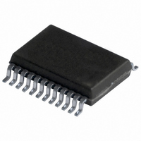
IC CLOCK DISTRIB 1:10 24SSOP
Manufacturer
NXP Semiconductors
Type
Fanout Buffer (Distribution)r
Datasheet
1.PCK351D112.pdf
(18 pages)
Specifications of PCK351DB,112
Package / Case
24-SSOP
Mounting Type
Surface Mount
Voltage - Supply
3 V ~ 3.6 V
Frequency-max
125MHz
Operating Temperature
-40°C ~ 85°C
Output
LVTTL
Number Of Circuits
1
Input
LVTTL
Ratio - Input:output
1:10
Differential - Input:output
No/No
Number Of Outputs
10
Propagation Delay (max)
4.1 ns
Supply Voltage (max)
3.6 V
Supply Voltage (min)
3 V
Maximum Power Dissipation
1700 mW
Maximum Operating Temperature
+ 85 C
Minimum Operating Temperature
- 40 C
Mounting Style
SMD/SMT
Lead Free Status / RoHS Status
Lead free / RoHS Compliant
Other names
935271531112::PCK351DB::PCK351DB
Available stocks
Company
Part Number
Manufacturer
Quantity
Price
Company:

Part Number:
PCK351DB,112
Manufacturer:
Maxim
Quantity:
49


Philips Semiconductors
6. Pinning information
PCK351_2
Product data sheet
6.1 Pinning
6.2 Pin description
Table 3:
Symbol
GND
Y10
Y9
Y8
Y7
Y6
Y5
Y4
Y3
Y2
Y1
V
OE
A
Fig 2. Pin configuration for SO24
CC
GND
GND
GND
GND
V
V
Y10
OE
CC
CC
Y9
Y8
Y7
A
Pin description
10
11
12
1
2
3
4
5
6
7
8
9
Pin
1, 7, 8, 12, 13, 17, 20, 24
2
4
9
11
14
16
18
19
21
23
3, 10, 15, 22
5
6
PCK351D
Rev. 02 — 16 December 2005
002aaa280
24
23
22
21
20
19
18
17
16
15
14
13
GND
Y1
V
Y2
GND
Y3
Y4
GND
Y5
V
Y6
GND
1 : 10 clock distribution device with 3-state outputs
CC
CC
Fig 3. Pin configuration for SSOP24
GND
GND
GND
GND
V
V
Y10
OE
CC
CC
Y9
Y8
Y7
A
Description
ground (0 V)
outputs
supply voltage
output enable input (active LOW)
data input
10
11
12
1
2
3
4
5
6
7
8
9
© Koninklijke Philips Electronics N.V. 2005. All rights reserved.
PCK351DB
002aaa281
PCK351
24
23
22
21
20
19
18
17
16
15
14
13
GND
Y1
V
Y2
GND
Y3
Y4
GND
Y5
V
Y6
GND
CC
CC
4 of 18
Related parts for PCK351DB,112
Image
Part Number
Description
Manufacturer
Datasheet
Request
R

Part Number:
Description:
Clock Buffer 1:10 CLK DISTR DEV 3-ST OUTPUT
Manufacturer:
NXP Semiconductors
Datasheet:
Part Number:
Description:
Clock Buffer 1:10 CLK DISTR DEV 3-ST OUTPUT
Manufacturer:
NXP Semiconductors
Datasheet:

Part Number:
Description:
IC CLOCK DISTRIB 1:10 24SSOP
Manufacturer:
NXP Semiconductors
Datasheet:
Part Number:
Description:
Clock Buffer 1:10 CLK DISTR DEV 3-ST OUTPUT
Manufacturer:
NXP Semiconductors
Datasheet:
Part Number:
Description:
Clock Buffer 1:10 CLK DISTR DEV 3-ST OUTPUT
Manufacturer:
NXP Semiconductors
Datasheet:

Part Number:
Description:
IC CLOCK DISTRIB 1:10 24SOIC
Manufacturer:
NXP Semiconductors
Datasheet:
Part Number:
Description:
IC CLOCK DISTRIB 1:10 24SOIC
Manufacturer:
NXP Semiconductors
Datasheet:

Part Number:
Description:
NXP Semiconductors designed the LPC2420/2460 microcontroller around a 16-bit/32-bitARM7TDMI-S CPU core with real-time debug interfaces that include both JTAG andembedded trace
Manufacturer:
NXP Semiconductors
Datasheet:

Part Number:
Description:
NXP Semiconductors designed the LPC2458 microcontroller around a 16-bit/32-bitARM7TDMI-S CPU core with real-time debug interfaces that include both JTAG andembedded trace
Manufacturer:
NXP Semiconductors
Datasheet:
Part Number:
Description:
NXP Semiconductors designed the LPC2468 microcontroller around a 16-bit/32-bitARM7TDMI-S CPU core with real-time debug interfaces that include both JTAG andembedded trace
Manufacturer:
NXP Semiconductors
Datasheet:
Part Number:
Description:
NXP Semiconductors designed the LPC2470 microcontroller, powered by theARM7TDMI-S core, to be a highly integrated microcontroller for a wide range ofapplications that require advanced communications and high quality graphic displays
Manufacturer:
NXP Semiconductors
Datasheet:
Part Number:
Description:
NXP Semiconductors designed the LPC2478 microcontroller, powered by theARM7TDMI-S core, to be a highly integrated microcontroller for a wide range ofapplications that require advanced communications and high quality graphic displays
Manufacturer:
NXP Semiconductors
Datasheet:
Part Number:
Description:
The Philips Semiconductors XA (eXtended Architecture) family of 16-bit single-chip microcontrollers is powerful enough to easily handle the requirements of high performance embedded applications, yet inexpensive enough to compete in the market for hi
Manufacturer:
NXP Semiconductors
Datasheet:
Part Number:
Description:
The XA-S3 device is a member of Philips Semiconductors? XA(eXtended Architecture) family of high performance 16-bitsingle-chip microcontrollers
Manufacturer:
NXP Semiconductors
Datasheet: