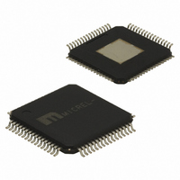
SY89828LHY Micrel Inc, SY89828LHY Datasheet - Page 6

SY89828LHY
Manufacturer Part Number
SY89828LHY
Description
IC BUFFER/XLATOR LVDS 64-TQFP
Manufacturer
Micrel Inc
Series
Precision Edge®r
Type
Fanout Buffer (Distribution), Multiplexer , Translatorr
Datasheet
1.SY89828LHY.pdf
(13 pages)
Specifications of SY89828LHY
Number Of Circuits
2
Ratio - Input:output
2:10
Differential - Input:output
Yes/Yes
Input
LVDS, PECL
Output
LVDS
Frequency - Max
1GHz
Voltage - Supply
3 V ~ 3.6 V
Operating Temperature
-40°C ~ 85°C
Mounting Type
Surface Mount
Package / Case
64-TQFP Exposed Pad, 64-eTQFP, 64-HTQFP, 64-VQFP
Frequency-max
1GHz
Number Of Clock Inputs
4
Mode Of Operation
Differential
Output Frequency
1000MHz
Output Logic Level
LVDS
Operating Supply Voltage (min)
3V
Operating Supply Voltage (typ)
3.3V
Operating Supply Voltage (max)
3.6V
Package Type
TQFP EP
Operating Temp Range
-40C to 85C
Operating Temperature Classification
Industrial
Signal Type
LVDS/LVPECL
Mounting
Surface Mount
Pin Count
64
Lead Free Status / RoHS Status
Lead free / RoHS Compliant
Other names
576-2091
SY89828LHY
SY89828LHY
Available stocks
Company
Part Number
Manufacturer
Quantity
Price
Company:
Part Number:
SY89828LHY
Manufacturer:
MICREL
Quantity:
506
Micrel, Inc.
Absolute Maximum Ratings
Power Supply Voltage (V
Input Voltage (V
Output Current (I
Storage Temperature (T
ESD Rating, Note 3 ...................................................... 1kV
Power Supply
Symbol
V
I
I
LVDS Input
Symbol
V
V
I
R
Note 1.
Note 2.
Note 3.
Note 4.
M9999-012208
hbwhelp@micrel.com or (408) 955-1690
CCI
CCO
IL
CCI
IN
ID
IN
DC ELECTRICAL CHARACTERISTICS
, V
CCO
Permanent device damage may occur if ABSOLUTE MAXIMUM RATINGS are exceeded. This is a stress rating only and functional operation
is not implied at conditions other than those detailed in the operational sections of this data sheet. Exposure to ABSOLUTE MAXIMUM RATlNG
The data sheet limits are not guaranteed if the device is operated beyond the operating ratings.
Devices are ESD sensitive. Handling precautions recommended.
V
connected on the die.
conditions for extended periods may affect device reliability.
CCI
: V
and V
Parameter
V
I
I
Parameter
Input Voltage Range
Differential Input Swing
Input LOW Current
LVDS Differential Input Resistance
(LVDS_CLK to /LVDS_CLK)
CC
CC
: T
CC
CC
IN
OUT
CCO
Core
Output
A
Core, V
) ........................................... –0.5 to V
= 3.3V ±10%, T
= –40°C to +85°C
) ............................................... ±10mA
must be connected together on the PCB such that they remain at the same potential. V
S
CC
CCI
) ........................... –65 to +150°C
Output
, V
CCO
A
= –40°C to +85°C
) .............. –0.5 to +4.0V
(Note 1)
Condition
Note 4
Max. V
No Load, Max. V
Condition
CC
CCI
6
Operating Ratings
Supply Voltage ............................................... +3V to +3.6V
Ambient Temperature (T
Package Thermal Resistance
CC
TQFP (θ
Exposed pad soldered to GND
Exposed pad NOT soldered to GND (not recommened)
TQFP (θ
Still-Air (multi-layer PCB) ................................. 23°C/W
–200lfpm (multi-layer PCB) ............................. 18°C/W
–500lfpm (multi-layer PCB) ............................. 15°C/W
Still-Air (multi-layer PCB) ................................. 44°C/W
–200lfpm (multi-layer PCB) ............................. 36°C/W
–500lfpm (multi-layer PCB) ............................. 30°C/W
JA
JC
)
) ......................................................... 4.4°C/W
A
(Note 2)
) ......................... –40°C to +85°C
CCI
–1.25
Min
Min
100
3.0
80
and V
0
CCO
Typ
Typ
160
100
3.3
45
are not internally
Precision Edge
Max
Max
260
120
3.6
2.4
70
SY89828L
Units
Units
mA
mA
mV
mA
Ω
V
V
®


