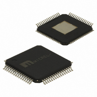
SY89828LHY Micrel Inc, SY89828LHY Datasheet - Page 12

SY89828LHY
Manufacturer Part Number
SY89828LHY
Description
IC BUFFER/XLATOR LVDS 64-TQFP
Manufacturer
Micrel Inc
Series
Precision Edge®r
Type
Fanout Buffer (Distribution), Multiplexer , Translatorr
Datasheet
1.SY89828LHY.pdf
(13 pages)
Specifications of SY89828LHY
Number Of Circuits
2
Ratio - Input:output
2:10
Differential - Input:output
Yes/Yes
Input
LVDS, PECL
Output
LVDS
Frequency - Max
1GHz
Voltage - Supply
3 V ~ 3.6 V
Operating Temperature
-40°C ~ 85°C
Mounting Type
Surface Mount
Package / Case
64-TQFP Exposed Pad, 64-eTQFP, 64-HTQFP, 64-VQFP
Frequency-max
1GHz
Number Of Clock Inputs
4
Mode Of Operation
Differential
Output Frequency
1000MHz
Output Logic Level
LVDS
Operating Supply Voltage (min)
3V
Operating Supply Voltage (typ)
3.3V
Operating Supply Voltage (max)
3.6V
Package Type
TQFP EP
Operating Temp Range
-40C to 85C
Operating Temperature Classification
Industrial
Signal Type
LVDS/LVPECL
Mounting
Surface Mount
Pin Count
64
Lead Free Status / RoHS Status
Lead free / RoHS Compliant
Other names
576-2091
SY89828LHY
SY89828LHY
Available stocks
Company
Part Number
Manufacturer
Quantity
Price
Company:
Part Number:
SY89828LHY
Manufacturer:
MICREL
Quantity:
506
Micrel, Inc.
allows either LVPECL or LVDS inputs, selectable by an
input muxes, and outputs 2 sets of 10 LVDS output pairs.
The device features 2 synchronous output enables. The
SY89828L provides extremely low skew across its outputs.
LVPECL_CLKA, LVPECL_CLKB
voltage swings. These inputs may be adjusted per the data
sheet characteristics regarding the CMR and minimum input
swing. As the SY89828L contains no appropriate internal
termination, upstream devices need to be properly
terminated to provide the proper LVPECL input swing. If
not being used (CLK_SEL1 and CLK_SEL2 are LOW), these
input pairs may be left floating, as they are internally
terminated to ground via 75kΩ pull-down resistors.
LVDS_CLKA, LVDS_CLKB
voltage swings. The SY89828L provides an appropriate
internal 100Ω termination resistor. Hence, upstream LVDS
devices do not require external termination to drive the
SY89828L. If not being used (CLK_SEL1 and CLK_SEL2
are HIGH), these inputs pair may be left floating.
SEL1, SEL2 TTL Inputs
LOW) or CLKB (SEL1 is HIGH) for the Q0-Q9 differential
output pairs. In a similar manner, The SEL2 Input is used to
select either CLKA (SEL2 is LOW)or CLKB (SEL2 is HIGH)
for the Q10-Q19 differential output pairs.
M9999-012208
hbwhelp@micrel.com or (408) 955-1690
Part Number
SY55855V
SY89825U
SY89826U
SY89829U
M-0317
Exposed pad
DETAILED DESCRIPTION
RELATED MICREL PRODUCTS AND SUPPORT DOCUMENTATION
The SY89828L is a precision dual 1:10 fanout buffer. It
The SY89828L allows two inputs with standard LVPECL
The SY89828L allows two inputs with standard LVDS
The SEL1 Input is used to select either CLKA (SEL1 is
Function
Dual CML/PECL/LVPECL-to-LVDS Translator
2.5/3.3V 1:22 High-Performance, Low-Voltage PECL
Bus Clock Driver & Translator w/Internal Termination
3.3V 1GHz Precision 1:22 LVDS Fanout Buffer
with 2:1 Input Mux
2.5/3.3V High-Performance, Dual 1:10 LVPECL Clock
Driver w/Internal Termination & Redundant Switchover
HBW Solutions
Amkor Exposed Pad Application Note
12
CLK_SEL1, CLK_SEL2 TTL Inputs
(CLK_SEL1 is LOW) or LVPECL_CLKA (CLK_SEL1 is
HIGH). In a similar manner, The CLK_SEL2 Input is used
to select either LVDS_CLKB (CLK_SEL2 is LOW) or
LVPECL_CLKB (CLK_SEL2 is HIGH).
OE1, OE2 TTL Inputs
disable the outputs only when the outputs are LOW. The
OE1 TTL Input controls the Q0-Q9 outputs and OE2 controls
the Q10-Q19 outputs. This avoids the possibility of
generating runt pulses. The OE1 and OE2 inputs are
asynchronous inputs, but operate as synchronous enables.
For synchronous operation, please adhere to the specific
setup and hold times. When disabled, the Q outputs are
LOW and the /Q outputs are HIGH.
Q0-Q9, Q10-Q19 LVDS Outputs
around a 1.25V common mode voltage above ground. The
common mode voltage has tight limits to permit large
variations in ground between an LVDS driver and receiver.
Also, change in common mode voltage, as a function of
data input is kept tight to keep EMI low. Each of the
SY89828L’s LVDS outputs should be terminated with a 100Ω
termination resistor including any unused output pairs. This
ensures the best jitter and skew performance of the device.
In a similar manner, The SEL2 Input is used to select either
CLKA (SEL2 is LOW)or CLKB (SEL2 is HIGH) for the Q10-
Q19 differential output pairs.
The CLK_SEL1 Input is used to select either LVDS_CLKA
The SY89828L’s output enable functions are designed to
The SY89828L’s LVDS outputs swing typically 350mV
Data Sheet Link
www.micrel.com/product-info/products/sy55855v.shtml
www.micrel.com/product-info/products/sy89825u.shtml
www.micrel.com/product-info/products/sy89826u.shtml
www.micrel.com/product-info/products/sy89829u.shtml
www.micrel.com/product-info/products/solutions.shtml
www.amkor.com/products/notes_papers/ePad.pdf
Precision Edge
SY89828L
®


