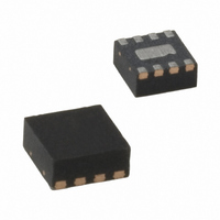
SY58605UMG TR Micrel Inc, SY58605UMG TR Datasheet - Page 2

SY58605UMG TR
Manufacturer Part Number
SY58605UMG TR
Description
IC BUFFER LVDS 3.2GBPS FSI 8-MLF
Manufacturer
Micrel Inc
Series
Precision Edge®r
Type
Buffer/Driverr
Datasheet
1.SY58605UMG_TR.pdf
(12 pages)
Specifications of SY58605UMG TR
Number Of Circuits
1
Ratio - Input:output
1:1
Differential - Input:output
Yes/Yes
Input
CML, LVDS, LVPECL
Output
LVDS
Frequency - Max
3GHz
Voltage - Supply
2.375 V ~ 2.625 V
Operating Temperature
-40°C ~ 85°C
Mounting Type
Surface Mount
Package / Case
8-MLF®, QFN
Frequency-max
3GHz
Number Of Outputs
2
Operating Supply Voltage (max)
2.625V
Operating Temp Range
-40C to 85C
Propagation Delay Time
0.42ns
Operating Supply Voltage (min)
2.375V
Mounting
Surface Mount
Pin Count
8
Operating Supply Voltage (typ)
2.5V
Package Type
MLF
Input Frequency
3GHz
Duty Cycle
53%
Operating Temperature Classification
Industrial
Lead Free Status / RoHS Status
Lead free / RoHS Compliant
Lead Free Status / RoHS Status
Compliant, Lead free / RoHS Compliant
Other names
576-1596-2
Micrel, Inc.
Ordering Information
Pin Configuration
Pin Description
August 2007
Notes:
1. Contact factory for die availability. Dice are guaranteed at T
2. Tape and Reel.
Part Number
SY58605UMG
SY58605UMGTR
Pin Number
1, 4
6, 7
2
3
5
8
(2)
Exposed pad
Pin Name
VREF-AC
IN, /IN
GND,
/Q, Q
VCC
(1)
VT
Package
DFN-8
DFN-8
Type
Pin Function
Differential Input: This input pair is the differential signal input to the device. Input
accepts DC-coupled differential signals as small as 100mV (200mV
this pair internally terminates with 50Ω to the VT pin. If the input swing falls below a
certain threshold (typically 30mV), them the Fail Safe Input (FSI) feature will
guarantee a stable output by latching the output to its last valid state. See “Input
Interface Applications” subsection for more details.
Input Termination Center-Tap: Each input terminates to this pin. The V
a center-tap for each input (IN, /IN) to a termination network for maximum interface
flexibility. See “Input Interface Applications” subsection for more details.
Reference Voltage: This output biases to V
IN and /IN. Connect VREF-AC directly to the VT pin. Bypass with 0.01µF low ESR
capacitor to VCC. Maximum sink/source current is ±1.5mA. See “Input Interface
Applications” subsection for more details.
Ground: Exposed pad must be connected to a ground plane that is the same
potential as the ground pin.
LVDS Differential Output Pair: The output swing is typically 325mV. Normally
terminated with 100Ω across the pair (Q, /Q). See “LVDS Output Termination”
subsection for more details.
Positive Power Supply: Bypass with 0.1µF//0.01µF low ESR capacitors as close to
the V
Operating
CC
Industrial
Industrial
Range
pin as possible.
8-Pin DFN
A
= 25°C, DC Electricals only.
2
Package Marking
605 with Pb-Free
605 with Pb-Free
bar-line indicator
bar-line indicator
CC
hbwhelp@micrel.com
–1.2V. It is used for AC-coupling input
Pb-Free
Pb-Free
NiPdAu
NiPdAu
Finish
Lead
or (408) 955-1690
M9999-082907-B
PP
). Each pin of
T
pin provides
SY58605U


