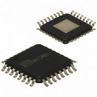
SY69753LHI TR Micrel Inc, SY69753LHI TR Datasheet

SY69753LHI TR
Specifications of SY69753LHI TR
SY69753LHITR
Related parts for SY69753LHI TR
SY69753LHI TR Summary of contents
Page 1
... The SY69753L also includes a link fault detection circuit. Datasheets and support documentation can be found on Micrel’s web site at: www.micrel.com. Micrel Inc. • 2180 Fortune Drive • San Jose, CA 95131 • USA • tel +1 (408) 944-0800 • fax + 1 (408) 474-1000 • http://www.micrel.com December 2007 SY69753L 3 ...
Page 2
Ordering Information Part Number Package Type SY69753LHI H32-1 (2) SY69753LHITR H32-1 (3) SY69753LHG H32-1 (2, 3) SY69753LHGTR H32-1 Notes: 1. Contact factory for die availability. Dice are guaranteed Tape and Reel. 3. Recommended for new designs. ...
Page 3
Pin Description Inputs Pin Number Pin Name Type 2 RDINP Differential 3 RDINN PECL 5 REFCLK TTL Input 26 CD PECL Input 32 DIVSEL1 TTL Input 25 DIVSEL2 16 CLKSEL TTL Input Outputs Pin Number Pin Name Type 31 LFIN ...
Page 4
Absolute Maximum Ratings Supply Voltage (V ) ......................................-0.5V to +5.0V CC Input Voltage (V ) ..............................................-0. Output Current (I ) OUT Continuous ...........................................................±50mA Surge..................................................................±100mA Lead Temperature (soldering, 20sec.) ..................... +260°C Storage Temperature (T ) .......................... -65°C to ...
Page 5
AC Electrical Characteristics 3.3V ±5 CCO CCA Symbol Parameter f VCO Center Frequency VCO VCO Center Frequency Δf VCO Tolerance t Acquisition Lock Time ACQ t REFCLK Pulse Width HIGH CPWH t ...
Page 6
Functional Block Functional Description Clock Recovery Clock Recovery, as shown in the block diagram, generates a clock that is at the same frequency as the incoming data bit rate at the Serial Data input. The clock is phase aligned by ...
Page 7
Input Jitter Tolerance Input jitter tolerance is defined as the peak-to-peak amplitude of sinusoidal jitter applied on the input signal that causes an equivalent 1dB optical/electrical power penalty. SONET input jitter tolerance requirement condition is the input jitter amplitude that ...
Page 8
Loop Filter Components R1 = 350Ω 1.5µF (X7R Dielectric) Note: 1. Suggested values. Values may vary for different applications. Reference Frequency Selection DIVSEL1 DIVSEL2 December 2007 ( RCLK ...
Page 9
Application Example Note: C3, C4 are optional 1.5µ 1.0µ 350Ω 680Ω R3 through R10 = 5kΩ R12 = 12kΩ R13 = 130Ω December 2007 9 hbwhelp@micrel.com M9999-120307-F or (408) 955-1690 ...
Page 10
Bill of Materials Item Part Number C1 ECU-V1H104KBW C2 ECU-V1H104KBW C3, C4 ECU-V1H104KBW C5 ECS-T1ED226R C6 ECU-V1H104KBW C7, C8, C9, C10 ECS-T1EC685R C19 ECJ-3YB1E105K C11, C13 ECU-V1H104KBW C15, C17 ECU-V1H104KBW C20 ECU-V1H104KBW C12, C14 ECU-V1H103KBW C16, C18 ECU-V1H103KBW C21 ECU-V1H103KBW ...
Page 11
Appendix A Layout and General Suggestions 1. Establish controlled impedance stripline, microstrip, or coplanar construction techniques. 2. Signal paths should have approximately the same width as the device pads. 3. All differential paths are critical timing paths, where skew should ...
Page 12
Package Information December 2007 32-Pin EPAD-TQFP (H32-1) 12 M9999-120307-F hbwhelp@micrel.com or (408) 955-1690 ...
Page 13
PCB Thermal Consideration for 32-Pin EPAD-TQFP Package MICREL, INC. 2180 FORTUNE DRIVE SAN JOSE, CA 95131 USA TEL +1 (408) 944-0800 FAX +1 (408) 474-1000 WEB http://www.micrel.com The information furnished by Micrel in this data sheet is believed to be ...


