NHD-2.7-12864UCY3 Newhaven Display, NHD-2.7-12864UCY3 Datasheet - Page 10
NHD-2.7-12864UCY3
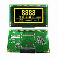
Manufacturer Part Number
NHD-2.7-12864UCY3
Description
LCD OLED GRAPHIC 128 X 64 YLW
Manufacturer
Newhaven Display
Datasheet
1.NHD-2.7-12864UCY3.pdf
(11 pages)
Specifications of NHD-2.7-12864UCY3
Pixel Density
128 x 64
Viewing Area (w X H)
66 mm x 33 mm
Operating Voltage
2.8 V
Operating Current
53 mA
Maximum Operating Temperature
+ 85 C
Minimum Operating Temperature
- 40 C
Illumination Color
Yellow
Viewing Angle
80 deg
Lead Free Status / Rohs Status
Lead free / RoHS Compliant


Serial Interface
The serial interface consists of serial clock SCLK, serial data SDIN, D/C, and /CS.
D0 acts as SCLK and D1 acts as SDIN. D2 should be left open. D3~D7, E, and R/W should be connected to GND.
SDIN is shifted into an 8‐bit shift register on every rising edge of SCLK in the order of D7, D6,…D0.
D/C is sampled on every eighth clock and the data byte in the shift register is written to the GDRAM or
command register in the same clock.
Note: Read is not available in serial mode.
For detailed protocol information, see datasheet: http://www.newhavendisplay.com/app_notes/SSD1325.pdf
Example Initialization Sequence:
Set_Display_On_Off_12864(0x00);
Set_Display_Clock_12864(0x91);
Set_Multiplex_Ratio_12864(0x3F);
Set_Display_Offset_12864(0x4C);
Set_Start_Line_12864(0x00);
Set_Master_Config_12864(0x00);
Set_Remap_Format_12864(0x50);
Set_Current_Range_12864(0x02);
Set_Gray_Scale_Table_12864();
Set_Contrast_Current_12864(brightness);
Set_Frame_Frequency_12864(0x51);
Set_Phase_Length_12864(0x55);
Set_Precharge_Voltage_12864(0x10);
Set_Precharge_Compensation_12864(0x20,0x02);
Set_VCOMH_12864(0x1C);
Set_VSL_12864(0x0D);
Set_Display_Mode_12864(0x00);
Fill_RAM_12864(0x00);
Set_Display_On_Off_12864(0x01);
Function
Write Command
Write Data
/RD /WR
0
0
0
0
/CS
0
0
// Display Off (0x00/0x01)
// Set Clock as 135 Frames/Sec
// 1/64 Duty (0x0F~0x5F)
// Shift Mapping RAM Counter (0x00~0x5F)
// Set Mapping RAM Display Start Line (0x00~0x5F)
// Disable Embedded DC/DC Converter (0x00/0x01)
// Set Column Address 0 Mapped to SEG0
// Disable Nibble Remap
// Horizontal Address Increment
// Scan from COM[N‐1] to COM0
// Enable COM Split Odd Even
// Set Full Current Range
// Set Pulse Width for Gray Scale Table
// Set Scale Factor of Segment Output Current Control
// Set Frame Frequency
// Set Phase 1 as 5 Clocks & Phase 2 as 5 Clocks
// Set Pre‐Charge Voltage Level
// Set High Voltage Level of COM Pin
// Set Low Voltage Level of SEG Pin
// Normal Display Mode (0x00/0x01/0x02/0x03)
// Clear Screen
// Display On (0x00/0x01)
[10]
D/C
0
1
// Set Pre‐Charge Compensation
D0
↑
↑
Related parts for NHD-2.7-12864UCY3
Image
Part Number
Description
Manufacturer
Datasheet
Request
R

Part Number:
Description:
LCD MOD CHAR 1X8 GRY TRANSFL
Manufacturer:
Newhaven Display
Datasheet:

Part Number:
Description:
LCD MOD CHAR 1X8 Y/G REFL
Manufacturer:
Newhaven Display
Datasheet:

Part Number:
Description:
LCD MOD CHAR 1X8 Y/G TRANSFL
Manufacturer:
Newhaven Display
Datasheet:

Part Number:
Description:
LCD COG CHAR 2X16 NO TRANSFL
Manufacturer:
Newhaven Display
Datasheet:

Part Number:
Description:
LCD MOD CHAR 2X24 WH TRANSFL
Manufacturer:
Newhaven Display
Datasheet:

Part Number:
Description:
LCD MOD CHAR 2X8 Y/G REFL
Manufacturer:
Newhaven Display
Datasheet:

Part Number:
Description:
LCD MOD CHAR 2X8 GRY REFL
Manufacturer:
Newhaven Display
Datasheet:

Part Number:
Description:
LCD COG CHAR 2X16 TRANSFL
Manufacturer:
Newhaven Display
Datasheet:

Part Number:
Description:
LCD MOD CHAR 2X8 TRANSF
Manufacturer:
Newhaven Display
Datasheet:

Part Number:
Description:
LCD MOD CHAR 4X20 TRANSFL
Manufacturer:
Newhaven Display
Datasheet:
Part Number:
Description:
LCD COG CHAR 2X16 NO TRANSFL
Manufacturer:
Newhaven Display
Datasheet:

Part Number:
Description:
Display Drivers & Controllers TFT Eval 20 POS FFC For NHD 5.0" TFT
Manufacturer:
Newhaven Display

Part Number:
Description:
TFT Displays & Accessories Digital Cont Brd w/ Touch Panel Input
Manufacturer:
Newhaven Display
Part Number:
Description:
TFT Displays & Accessories Digital Cont Brd For TFT
Manufacturer:
Newhaven Display
Datasheet:
Part Number:
Description:
TOUCH PANEL FOR 113X50MM LCD
Manufacturer:
Newhaven Display