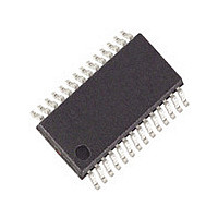
DS90LV110ATMT National Semiconductor, DS90LV110ATMT Datasheet - Page 6

DS90LV110ATMT
Manufacturer Part Number
DS90LV110ATMT
Description
Manufacturer
National Semiconductor
Datasheet
1.DS90LV110ATMT.pdf
(12 pages)
Specifications of DS90LV110ATMT
Number Of Elements
1
Input Type
CMOS/TTL
Operating Supply Voltage (typ)
3.3V
Differential Input High Threshold Voltage
100mV
Diff. Input Low Threshold Volt
-100mV
Output Type
Repeater
Differential Output Voltage
450mV
Transmission Data Rate
400Mbps
Propagation Delay Time
3.9ns
Power Dissipation
1.209W
Operating Temp Range
-40C to 85C
Operating Temperature Classification
Industrial
Mounting
Surface Mount
Pin Count
28
Package Type
TSSOP
Number Of Receivers
1
Number Of Drivers
10
Lead Free Status / RoHS Status
Not Compliant
Available stocks
Company
Part Number
Manufacturer
Quantity
Price
Part Number:
DS90LV110ATMT
Manufacturer:
NS/国半
Quantity:
20 000
Company:
Part Number:
DS90LV110ATMT/NOPB
Manufacturer:
NS
Quantity:
321
Company:
Part Number:
DS90LV110ATMTCX/NOPB
Manufacturer:
NS/TI
Quantity:
600
www.national.com
DS90LV110A Pin Descriptions
Application Information
INPUT FAIL-SAFE
The receiver inputs of the DS90LV110A have internal fail-safe
biasing for short, open, and teminated input conditions.
LVDS INPUTS TERMINATION
The LVDS Receiver input must have a 100Ω termination re-
sistor placed as close as possible across the input pins.
UNUSED CONTROL INPUTS
The EN control input pin has internal pull down device. If left
open, the 10 outputs will default to TRI-STATE.
EXPANDING THE NUMBER OF OUTPUT PORTS
To expand the number of output ports, more than one
DS90LV110A can be used. Total propagation delay through
the devices should be considered to determine the maximum
expansion. Adding more devices will increase the output jitter
due to each pass.
PCB LAYOUT AND POWER SYSTEM BYPASS
Circuit board layout and stack-up for the DS90LV110A should
be designed to provide noise-free power to the device. Good
layout practice also will separate high frequency or high level
inputs and outputs to minimize unwanted stray noise pickup,
feedback and interference. Power system performance may
be greatly improved by using thin dielectrics (4 to 10 mils) for
power/ground sandwiches. This increases the intrinsic ca-
pacitance of the PCB power system which improves power
supply filtering, especially at high frequencies, and makes the
Pin Name
OUT -
OUT+
IN -
V
V
IN+
EN
DD
SS
# of Pin
10
10
1
1
1
3
2
Input/Output
O
O
P
P
I
I
I
6
Non-inverting LVDS input
Inverting LVDS input
Non-inverting LVDS Output
Inverting LVDS Output
This pin has an internal pull-down when left open. A logic
low on the Enable puts all the LVDS outputs into TRI-
STATE and reduces the supply current.
Ground (all ground pins must be tied to the same supply)
Power Supply (all power pins must be tied to the same
supply)
value and placement of external bypass capacitors less criti-
cal. External bypass capacitors should include both RF ce-
ramic and tantalum electrolytic types. RF capacitors may use
values in the range 0.01 µF to 0.1 µF. Tantalum capacitors
may be in the range 2.2 µF to 10 µF. Voltage rating for tan-
talum capacitors should be at least 5X the power supply
voltage being used. It is recommended practice to use two
vias at each power pin of the DS90LV110A as well as all RF
bypass capacitor terminals. Dual vias reduce the interconnect
inductance by up to half, thereby reducing interconnect in-
ductance and extending the effective frequency range of the
bypass components.
The outer layers of the PCB may be flooded with additional
ground plane. These planes will improve shielding and isola-
tion as well as increase the intrinsic capacitance of the power
supply plane system. Naturally, to be effective, these planes
must be tied to the ground supply plane at frequent intervals
with vias. Frequent via placement also improves signal in-
tegrity on signal transmission lines by providing short paths
for image currents which reduces signal distortion. The
planes should be pulled back from all transmission lines and
component mounting pads a distance equal to the width of
the widest transmission line or the thickness of the dielectric
separating the transmission line from the internal power or
ground plane(s) whichever is greater. Doing so minimizes ef-
fects on transmission line impedances and reduces unwanted
parasitic capacitances at component mounting pads.
There are more common practices which should be followed
when designing PCBs for LVDS signaling. Please see Appli-
cation Note: AN-1108 for additional information.
Description


