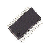
DS90LV110ATMT National Semiconductor, DS90LV110ATMT Datasheet - Page 2

DS90LV110ATMT
Manufacturer Part Number
DS90LV110ATMT
Description
Manufacturer
National Semiconductor
Datasheet
1.DS90LV110ATMT.pdf
(12 pages)
Specifications of DS90LV110ATMT
Number Of Elements
1
Input Type
CMOS/TTL
Operating Supply Voltage (typ)
3.3V
Differential Input High Threshold Voltage
100mV
Diff. Input Low Threshold Volt
-100mV
Output Type
Repeater
Differential Output Voltage
450mV
Transmission Data Rate
400Mbps
Propagation Delay Time
3.9ns
Power Dissipation
1.209W
Operating Temp Range
-40C to 85C
Operating Temperature Classification
Industrial
Mounting
Surface Mount
Pin Count
28
Package Type
TSSOP
Number Of Receivers
1
Number Of Drivers
10
Lead Free Status / RoHS Status
Not Compliant
Available stocks
Company
Part Number
Manufacturer
Quantity
Price
Part Number:
DS90LV110ATMT
Manufacturer:
NS/国半
Quantity:
20 000
Company:
Part Number:
DS90LV110ATMT/NOPB
Manufacturer:
NS
Quantity:
321
Company:
Part Number:
DS90LV110ATMTCX/NOPB
Manufacturer:
NS/TI
Quantity:
600
www.national.com
LVCMOS/LVTTL DC SPECIFICATIONS (EN)
V
V
I
I
V
LVDS OUTPUT DC SPECIFICATIONS (OUT1, OUT2, OUT3, OUT4, OUT5, OUT6, OUT7, OUT8, OUT9, OUT10)
V
ΔV
V
ΔV
I
I
I
I
LVDS RECEIVER DC SPECIFICATIONS (IN)
V
V
V
I
IH
IL
OZ
OFF
SA
SAB
IN
Symbol
IH
IL
CL
OD
OS
TH
TL
CMR
Absolute Maximum Ratings
If Military/Aerospace specified devices are required,
please contact the National Semiconductor Sales Office/
Distributors for availability and specifications.
Electrical Characteristics
Over recommended operating supply and temperature ranges unless otherwise specified
,I
Supply Voltage (V
LVCMOS/LVTTL Input Voltage
(EN)
LVDS Receiver Input Voltage
(IN+, IN−)
LVDS Driver Output Voltage
(OUT+, OUT−)
Junction Temperature
Storage Temperature Range
Lead Temperature
Maximum Package Power Dissipation at 25°C
OD
OS
SB
28L TSSOP
(Soldering, 4 sec.)
High Level Input Voltage
Low Level Input Voltage
High Level Input Current
Low Level Input Current
Input Clamp Voltage
Differential Output Voltage
Change in V
Offset Voltage (Note 3)
Change in V
Output TRI-STATE Current
Power-Off Leakage Current
Output Short Circuit Current
Both Outputs Shorted (Note 4)
Differential Input High Threshold
Differential Input Low Threshold
Common Mode Voltage Range
Input Current
DD
-V
OD
OS
SS
Parameter
between Complimentary Output States
)
between Complimentary Output States
−0.3V to (V
−65°C to +150°C
−0.3V to +4V
−0.3V to +4V
−0.3V to +4V
(Note 1)
CC
2.115 W
+150°C
+260°C
+ 0.3V)
V
V
I
R
R
EN = 0V,
V
V
V
V
V
V
V
V
V
CL
IN
IN
OUT
DD
OUT+
OUT+
CM
DD
ID
IN
IN
L
L
= 100Ω
= 100Ω, V
= −18 mA
= 3.6V or 2.0V; V
= 0V or 0.8V; V
= 100mV, V
= +3.0V, V
= 0V, V
= 0V; V
= 3.3V
= +0.05V or +1.2V or +3.25V,
= V
OR V
= V
DD
OUT−
2
DD
or GND
OUT
OUT−
DD
= 3.6V or 0V
DD
Conditions
Recommended Operating
Conditions
DD
= 3.6V or GND
Package Derating
θ
(4-Layer, 2 oz. Cu, JEDEC)
ESD Rating:
Supply Voltage (V
Receiver Input Voltage
Operating Free Air Temperature
= 3.3V, T
= 0V or V
JA
= 3.6V or 0V
28L TSSOP
28L TSSOP
(HBM, 1.5kΩ, 100pF)
(EIAJ, 0Ω, 200pF)
= 3.3V
DD
DD
= 3.6V
= 3.6V
A
DD
= 25°C
DD
- V
SS
)
1.125
−100
0.05
Min
V
250
260
2.0
SS
16.9 mW/°C above +25°C
Min Typ Max Units
3.0
-40 +25 +85
0
−0.8
1.25
Typ
320
320
±7
±7
±1
±1
12
±1
±1
6
0
0
3.3
59.1 °C/Watt
1.375
+100
Max
−1.5
3.25
V
±20
±20
450
425
±10
±10
±10
±10
0.8
V
35
35
24
12
3.6
DD
DD
> 250 V
> 8 kV
°C
V
V
Units
|mV|
|mV|
|mA|
|mA|
mV
mV
mV
mV
μA
μA
μA
μA
μA
μA
V
V
V
V
V


