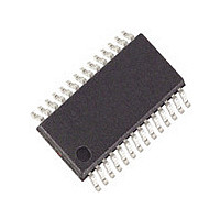
DS90LV110ATMT National Semiconductor, DS90LV110ATMT Datasheet

DS90LV110ATMT
Specifications of DS90LV110ATMT
Available stocks
Related parts for DS90LV110ATMT
DS90LV110ATMT Summary of contents
Page 1
... The LVDS outputs can be put into TRI-STATE enable pin. For more details, please refer to the Application Information section of this datasheet. Connection Diagram Order Number DS90LV110ATMT See NS Package Number MTC28 TRI-STATE ® registered trademark of National Semiconductor Corporation. © 2008 National Semiconductor Corporation Features ■ ...
Page 2
... Absolute Maximum Ratings If Military/Aerospace specified devices are required, please contact the National Semiconductor Sales Office/ Distributors for availability and specifications. Supply Voltage ( LVCMOS/LVTTL Input Voltage (EN) LVDS Receiver Input Voltage (IN+, IN−) LVDS Driver Output Voltage (OUT+, OUT−) Junction Temperature Storage Temperature Range Lead Temperature (Soldering, 4 sec ...
Page 3
Symbol Parameter SUPPLY CURRENT I Total Supply Current CCD I TRI-STATE Supply Current CCZ Note 1: “Absolute Maximum Ratings” are these beyond which the safety of the device cannot be guaranteed. They are not meant to imply that the device ...
Page 4
AC Timing Diagrams FIGURE 1. Output active to TRI-STATE and TRI-STATE to active output time www.national.com FIGURE 2. LVDS Driver TRI-STATE Circuit FIGURE 3. LVDS Output Load FIGURE 4. LVDS Output Transition Time 4 20098204 20098215 20098206 20098209 ...
Page 5
FIGURE 5. Propagation Delay Low-to-High and High-to-Low FIGURE 6. Output Channel-to-Channel Skew 5 20098207 20098208 www.national.com ...
Page 6
DS90LV110A Pin Descriptions Pin Name # of Pin IN OUT+ 10 OUT - Application Information INPUT FAIL-SAFE The receiver inputs of the DS90LV110A have internal fail-safe biasing ...
Page 7
INPUT INTERFACING The DS90LV110A accepts differential signals and allow sim- ple coupling. With a wide common mode range, the DS90LV110A can be DC-coupled with all common differential Typical LVDS Driver DC-Coupled Interface to DS90LV110A Input Typical CML ...
Page 8
OUTPUT INTERFACING The DS90LV110A outputs signals that are compliant to the LVDS standard. Their outputs can be DC-coupled to most common differential receivers. The following figure illustrates typical DC-coupled interface to common differential receivers Typical DS90LV110A Output DC-Coupled Interface to ...
Page 9
Multi-Drop Applications Point-to-Point Distribution Applications For applications operating at data rate greater than 400Mbps, a point-to-point distribution application should be used. This improves signal quality compared to multi-drop applications due to no stub PCB trace loading. The only load is ...
Page 10
Typical Performance Characteristics Output Voltage (V ) vs. Resistive Load (R OD Peak-to-Peak Output Jitter at V www.national.com ) Peak-to-Peak Output Jitter 20098211 = +1.2V vs. VID Peak-to-Peak Output Jitter 20098213 10 = +0.4V ...
Page 11
... Physical Dimensions inches (millimeters) unless otherwise noted Order Number DS90LV110ATMT (Rail quantity of 48) NS Package Number MTC28 DS90LV110ATMTX (2500 piece Tape and Reel) 11 www.national.com ...
Page 12
... For more National Semiconductor product information and proven design tools, visit the following Web sites at: Products Amplifiers www.national.com/amplifiers Audio www.national.com/audio Clock Conditioners www.national.com/timing Data Converters www.national.com/adc Displays www.national.com/displays Ethernet www.national.com/ethernet Interface www.national.com/interface LVDS www.national.com/lvds Power Management www.national.com/power Switching Regulators www.national.com/switchers LDOs www ...


