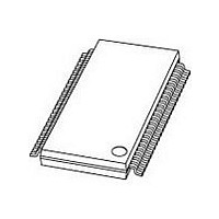
SSTVF16857DGG NXP Semiconductors, SSTVF16857DGG Datasheet - Page 8

SSTVF16857DGG
Manufacturer Part Number
SSTVF16857DGG
Description
Manufacturer
NXP Semiconductors
Datasheet
1.SSTVF16857DGG.pdf
(13 pages)
Specifications of SSTVF16857DGG
Logic Family
SSTV
Logical Function
Registered Buffer
Number Of Elements
1
Number Of Bits
14
Number Of Inputs
14
Number Of Outputs
14
High Level Output Current
-20mA
Low Level Output Current
20mA
Propagation Delay Time
1.9ns
Operating Supply Voltage (typ)
2.5V
Operating Supply Voltage (max)
2.7V
Operating Supply Voltage (min)
2.3V
Clock-edge Trigger Type
Posit/Negat-Edge
Polarity
Non-Inverting
Technology
CMOS
Frequency (max)
200(Min)MHz
Mounting
Surface Mount
Pin Count
48
Operating Temp Range
0C to 70C
Operating Temperature Classification
Commercial
Lead Free Status / RoHS Status
Compliant
Available stocks
Company
Part Number
Manufacturer
Quantity
Price
Philips Semiconductors
PARAMETER MEASUREMENT INFORMATION
AC WAVEFORMS
TEST CIRCUIT
2003 Sep 19
OUTPUT
CLK
DDR PC1600-PC3200 14-bit SSTL_2
registered driver with differential clock inputs
RESET
NOTES:
C
All input pulses are supplied by generators having the following characteristics:
PRR ≤ 10 MHz, Z
The outputs are measured one at a time with one transition per measurement.
V
OUTPUT
TT
L
includes probe and jig capacitance
Waveform 2. Propagation delay RESET to output.
= V
REF
Waveform 1. Propagation delay times
= V
t
PLH
V
DDQ
REF
O
= 50 Ω, t
x 0.5
V
V
REF
Figure 1. Load circuitry
REF
t
PHL
r
≤ 1.25 ns/V, t
V
REF
V
TT
f
1.25 ns/V.
TEST POINT
C
50 Ω
L
= 30 pF
t
PHL
V
REF
V
REF
SW00836
SW00837
SW00838
V
V
V
V
IH
OH
IL
OL
V
V
V
V
IH
IL
OH
OL
8
INPUT
TIMING INPUT
DATA INPUT
Waveform 4. Setup and hold times
V
REF
Waveform 3. Pulse duration
V
REF
t
t
W
su
V
REF
t
h
V
REF
SSTVF16857
V
REF
SW00339
Product data
SW00340
V
V
V
V
V
V
IH
IH
IH
IL
IL
IL


