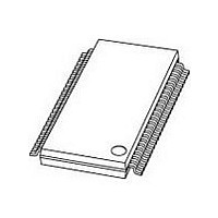
SSTV16857DGG NXP Semiconductors, SSTV16857DGG Datasheet - Page 5

SSTV16857DGG
Manufacturer Part Number
SSTV16857DGG
Description
Manufacturer
NXP Semiconductors
Datasheet
1.SSTV16857DGG.pdf
(12 pages)
Specifications of SSTV16857DGG
Logic Family
SSTV
Logical Function
Registered Buffer
Number Of Elements
1
Number Of Bits
14
Number Of Inputs
14
Number Of Outputs
14
High Level Output Current
-20mA
Low Level Output Current
20mA
Propagation Delay Time
2.4ns
Operating Supply Voltage (typ)
2.5V
Operating Supply Voltage (max)
2.7V
Operating Supply Voltage (min)
2.3V
Clock-edge Trigger Type
Posit/Negat-Edge
Polarity
Non-Inverting
Technology
CMOS
Frequency (max)
200MHz
Mounting
Surface Mount
Pin Count
48
Operating Temp Range
0C to 70C
Operating Temperature Classification
Commercial
Lead Free Status / RoHS Status
Compliant
1. Unused control inputs must be held HIGH or LOW to prevent them from floating.
1. When CLK and CLK are HIGH, typical I
2. All typical values are at V
Philips Semiconductors
RECOMMENDED OPERATING CONDITIONS
NOTE:
DC ELECTRICAL CHARACTERISTICS
Over recommended operating conditions. Voltages are referenced to GND (ground = 0 V).
NOTES:
2002 Sep 27
SYMBOL
SYMBOL
14-bit SSTL_2 registered driver
with differential clock inputs
V
V
V
T
V
V
V
V
V
V
V
V
I
I
V
V
I
CMR
V
V
I
DDQ
CC
CC
REF
amb
V
OH
OL
OH
O
OL
PP
I
CC
TT
IK
IH
IH
I
IL
IL
I
I/O supply voltage
HIGH level output voltage
HIGH level output voltage
LOW level output voltage
LOW level output voltage
CLK, CLK
CLK, CLK
Data inputs RESET
Data inputs, RESET
CLK CLK
CLK, CLK
V
Quiescent supply current
CLK and CLK in opposite
CLK and CLK in opposite
state
REF
Operating free-air temperature range
1
AC HIGH-level input voltage
DC HIGH-level input voltage
DC LOW-level input voltage
AC LOW-level input voltage
PARAMETER
HIGH-level output current
LOW-level output current
Output supply voltage
(V
Termination voltage
Reference voltage
REF
Supply voltage
PARAMETER
Input voltage
CC
= 0.5 x V
= 2.5 V and T
DDQ
CC
)
V
V
V
V
V
V
Common mode range for reliable performance
Minimum peak-to-peak input to ensure logic state
V
V
V
V
V
V
V
CC
CC
CC
CC
CC
CC
CC
CC
CC
CC
CC
CC
amb
= 25 mA.
= 2.7 V; V
= 2.7 V; V
= 2.7 V; V
= 2.7 V; V
= 2.7 V
= 2.7 V; V
= 2.7 V; V
= 2.3 V; I
= 2.3 V to 2.7 V; I
= 2 3 V; I
= 2.3 V; I
= 2.3 V to 2.7 V; I
= 2.3 V; I
= 25 C (unless otherwise specified).
I
OH
OL
TEST CONDITIONS
I
I
I
I
I
I
1
= –18 mA
= 1.7 V or 0.8 V
= 2.7 V or 0 V
= 1.7 V or 0.8 V
= 2.7 V or 0 V
= 1.7 V or 0.8 V
= 2.7 V or 0 V
= 16 mA
= 16 mA
= –16 mA
TEST CONDITIONS
All inputs
All inputs
All inputs
All inputs
OH
OL
= 100 A
= –100 A
5
V
V
V
V
V
RESET = GND
RESET = V
REF
REF
REF
V
V
= 1 15 V or 1 35 V
= 1.15 V or 1.35 V
= 1 15 V or 1 35 V
= 1.15 V or 1.35 V
= 1.15 V or 1.35 V
V
REF
REF
V
REF
SS
1.15
CC
MIN
+ 350 mV
+ 180 mV
2.3
2.3
– 40 mV
– 0.5 V
—
—
—
0
0
V
TYP
1.25
2.5
2.5
V
REF
—
—
—
—
—
—
—
—
CC
1 95
1.95
0.97
MIN
360
Temp = 0 to +70 C
—
—
—
—
—
—
—
—
—
—
– 0.2
V
V
V
V
LIMITS
REF
REF
REF
DDQ
SSTV16857
TYP
MAX
0.01
0.01
0.05
0.05
0.05
1.35
V
0.5
– 350 mV
– 180 mV
–20
—
—
—
—
—
—
—
10
2.7
2.7
+ 40 mV
20
70
—
CC
+ 0.5 V
2
MAX
–1.2
0.35
1.53
0.2
—
—
—
10
25
Product data
5
5
5
5
5
UNIT
mA
mA
UNIT
V
V
V
V
V
V
V
V
V
mV
mA
C
V
V
V
V
A
A
A
A
A
A


