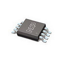
PCA9600DP-T NXP Semiconductors, PCA9600DP-T Datasheet - Page 3

PCA9600DP-T
Manufacturer Part Number
PCA9600DP-T
Description
Manufacturer
NXP Semiconductors
Datasheet
1.PCA9600DP-T.pdf
(30 pages)
Specifications of PCA9600DP-T
Operating Temperature (max)
85C
Operating Temperature (min)
-40C
Package Type
TSSOP
Pin Count
8
Mounting
Surface Mount
Lead Free Status / RoHS Status
Compliant
NXP Semiconductors
6. Pinning information
7. Functional description
PCA9600_4
Product data sheet
6.1 Pinning
6.2 Pin description
Table 3.
Refer to
The PCA9600 has two identical buffers allowing buffering of SDA and SCL I
signals. Each buffer is made up of two logic signal paths, a forward path from the I
interface, pins SX and SY which drive the buffered bus, and a reverse signal path from the
buffered bus input, pins RX and RY to drive the I
The rest of this discussion will address only the ‘X’ side of the buffer; the ‘Y’ side is
identical.
The I
systems.
Symbol
SX
RX
TX
GND
TY
RY
SY
V
Fig 2.
•
•
CC
sense the voltage state of I
(and TY respectively), and
sense the state of pins RX and RY and pull the I
pin RY is LOW.
2
C-bus pin SX is specified to allow interfacing with Fast-mode, Fm+ and TTL-based
Figure 1 “Block diagram of
GND
Pin configuration for SO8
SX
RX
TX
Pin description
1
2
3
4
Pin
1
2
3
4
5
6
7
8
PCA9600D
Rev. 04 — 11 November 2009
002aac836
Description
I
receive signal
transmit signal
negative supply voltage
transmit signal
receive signal
I
positive supply voltage
2
2
8
7
6
5
C-bus (SDA or SCL)
C-bus (SDA or SCL)
2
C-bus pins SX (and SY) and transmit this state to pin TX
V
SY
RY
TY
CC
PCA9600”.
Fig 3.
2
C-bus interface. These paths:
2
GND
C-bus pin LOW whenever pin RX or
RX
Pin configuration for TSSOP8
(MSOP8)
SX
TX
1
2
3
4
Dual bidirectional bus buffer
PCA9600DP
002aac837
PCA9600
© NXP B.V. 2009. All rights reserved.
8
7
6
5
2
C-bus
V
SY
RY
TY
CC
2
C-bus
3 of 30


