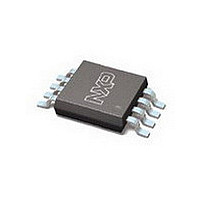
PCA9600DP-T NXP Semiconductors, PCA9600DP-T Datasheet - Page 14

PCA9600DP-T
Manufacturer Part Number
PCA9600DP-T
Description
Manufacturer
NXP Semiconductors
Datasheet
1.PCA9600DP-T.pdf
(30 pages)
Specifications of PCA9600DP-T
Operating Temperature (max)
85C
Operating Temperature (min)
-40C
Package Type
TSSOP
Pin Count
8
Mounting
Surface Mount
Lead Free Status / RoHS Status
Compliant
NXP Semiconductors
PCA9600_4
Product data sheet
Fig 15. Falling edge of SCL at master is delayed by the buffers and bus fall times
Fig 16. Rising edge of SCL at master is delayed (clock stretch) by buffer and bus rise times
V
CCM
MASTER
Effective delay of SCL at slave: 120 + 17V
C = F; V = V.
Effective delay of SCL at master: 115 + (Rm
C = F; R = .
I
2
C-BUS
local master bus
10.1 Calculating system delays and bus clock frequency
GND (0 V)
SCL
V
CCM
MASTER
I
2
C-BUS
Rm
Cm
master bus
capacitance
local master bus
GND (0 V)
V
SX
CCB
SCL
PCA9600
CCM
Rev. 04 — 11 November 2009
+ (2.5 + 4
Cm) + (0.7
TX/RX
Rm
buffered expansion bus
Cm
master bus
capacitance
V
SX
CCB
10
Cb
buffered bus
wiring capacitance
Rb
Rb
PCA9600
9
TX/RX
C
Cb) (ns).
b
)
buffered expansion bus
PCA9600
V
CCB
TX/RX
+ 10V
SX
CCS
Rb
Cb
buffered bus
wiring capacitance
(ns).
TX/RX
Dual bidirectional bus buffer
002aac848
Rs
Cs
slave bus
capacitance
remote slave bus
SCL
PCA9600
© NXP B.V. 2009. All rights reserved.
I
2
C-BUS
SLAVE
002aac847
V
CCS
14 of 30


