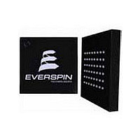
MR4A16BMA35 EverSpin Technologies Inc, MR4A16BMA35 Datasheet - Page 11

MR4A16BMA35
Manufacturer Part Number
MR4A16BMA35
Description
Manufacturer
EverSpin Technologies Inc
Datasheet
1.MR4A16BMA35.pdf
(15 pages)
Specifications of MR4A16BMA35
Word Size
16b
Density
16Mb
Interface Type
Parallel
Access Time (max)
35ns
Operating Supply Voltage (typ)
3.3V
Operating Temperature Classification
Commercial
Operating Supply Voltage (max)
3.6V
Operating Supply Voltage (min)
3V
Operating Temp Range
0C to 70C
Pin Count
48
Mounting
Surface Mount
Lead Free Status / RoHS Status
Compliant
Available stocks
Company
Part Number
Manufacturer
Quantity
Price
Company:
Part Number:
MR4A16BMA35
Manufacturer:
Everspin Technologies Inc
Quantity:
10 000
Part Number:
MR4A16BMA35
Manufacturer:
EVERSPIN
Quantity:
20 000
Company:
Part Number:
MR4A16BMA35R
Manufacturer:
Everspin Technologies Inc
Quantity:
10 000
Everspin Technologies © 2010
Timing Specifications
1
2
All write cycle timings are referenced from the last valid address to the first transition address.
Parameter
Write cycle time
Address set-up time
Address valid to end of write (G high)
Address valid to end of write (G low)
Write pulse width (G high)
Write pulse width (G low)
Data valid to end of write
Data hold time
Write recovery time
All write occurs during the overlap of E low and W low. Power supplies must be properly grounded and decoupled and bus
contention conditions must be minimized or eliminated during read and write cycles. If G goes low at the same time or after
W goes low, the output will remain in a high impedance state. After W, E or UB/LB has been brought high, the signal must
remain in steady-state high for a minimum of 2 ns. If both byte control signals are asserted, the two signals must have no
more than 2 ns skew between them. The minimum time between E being asserted low in one cycle to E being asserted low in
a subsequent cycle is the same as the minimum cycle time allowed for the device.
UB, LB (BYTE ENABLED)
W (WRITE ENABLE)
E (CHIP ENABLE)
Q (DATA OUT)
A (ADDRESS)
D (DATA IN)
2
Table 3.6 Write Cycle Timing 3 (LB/UB Controlled)
Figure 3.6 Write Cycle Timing 3 (LB/UB Controlled)
Hi -Z
t
AVBL
t
AVEH
11
Symbol
t
t
t
t
t
t
t
t
t
t
t
AVAV
AVBL
AVBH
AVBH
BLEH
BLWH
BLEH
BLWH
DVBH
BHDX
BHAX
t
AVAV
t
t
BLEH
BLWH
Document Number: MR4A16B Rev. 5, 4/2010
Hi -Z
Min
35
0
20
20
15
15
10
0
12
t
DVBH
Data Valid
1
Max
-
-
-
-
-
-
-
-
-
t
t
BHDX
BHAX
MR4A16B
Unit
ns
ns
ns
ns
ns
ns
ns
ns
ns


