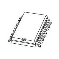
PCA9534D,112 NXP Semiconductors, PCA9534D,112 Datasheet - Page 6

PCA9534D,112
Manufacturer Part Number
PCA9534D,112
Description
Manufacturer
NXP Semiconductors
Datasheet
1.PCA9534D112.pdf
(25 pages)
Specifications of PCA9534D,112
Operating Temperature (min)
-40C
Operating Temperature Classification
Industrial
Operating Temperature (max)
85C
Package Type
SO
Rad Hardened
No
Lead Free Status / RoHS Status
Compliant
NXP Semiconductors
PCA9534_3
Product data sheet
6.1.5 Register 3 - Configuration register
6.2 Power-on reset
6.3 Interrupt output
6.4 I/O port
This register configures the directions of the I/O pins. If a bit in this register is set, the
corresponding port pin is enabled as an input with high-impedance output driver. If a bit in
this register is cleared, the corresponding port pin is enabled as an output. At reset, the
I/Os are configured as inputs.
Table 7.
Legend: * default value.
When power is applied to V
a reset condition until V
and the PCA9534 registers and state machine will initialize to their default states.
Thereafter, V
For a power reset cycle, V
operating voltage.
The open-drain interrupt output is activated when one of the port pins change state and
the pin is configured as an input. The interrupt is deactivated when the input returns to its
previous state or the Input Port register is read.
Note that changing an I/O from and output to an input may cause a false interrupt to occur
if the state of the pin does not match the contents of the Input Port register.
When an I/O is configured as an input, FETs Q1 and Q2 are off, creating a
high-impedance input. The input voltage may be raised above V
If the I/O is configured as an output, then either Q1 or Q2 is enabled, depending on the
state of the Output Port register. Care should be exercised if an external voltage is applied
to an I/O configured as an output because of the low-impedance paths that exist between
the pin and either V
Bit
7
6
5
4
3
2
1
0
Symbol
C7
C6
C5
C4
C3
C2
C1
C0
Register 3 - Configuration register bit description
DD
must be lowered below 0.2 V to reset the device.
DD
Access
R/W
R/W
R/W
R/W
R/W
R/W
R/W
R/W
Rev. 03 — 6 November 2006
or V
DD
DD
has reached V
SS
DD
8-bit I
.
must be lowered below 0.2 V and then restored to the
, an internal Power-On Reset (POR) holds the PCA9534 in
Value
1*
1*
1*
1*
1*
1*
1*
1*
2
C-bus and SMBus low power I/O port with interrupt
POR
Description
configures the directions of the I/O pins
0 = corresponding port pin enabled as an output
1 = corresponding port pin configured as input
(default value)
. At that point, the reset condition is released
DD
to a maximum of 5.5 V.
PCA9534
© NXP B.V. 2006. All rights reserved.
6 of 25


