JL198SGA National Semiconductor, JL198SGA Datasheet
JL198SGA
Specifications of JL198SGA


Related parts for JL198SGA

JL198SGA Summary of contents
Page 1
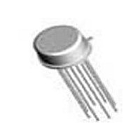
... Ordering Information NSC Part Number JAN Part Number JL198BGA JM38510/12501BGA JL198SGA JM38510/12501SGA Connection Diagrams © 2005 National Semiconductor Corporation Features n Operates from n Less than 10 µs acquisition time n TTL, PMOS, CMOS compatible logic input n 0 ...
Page 2
Typical Connection and Performance Curve Functional Diagram www.national.com Acquisition Time 20128132 2 20128116 20128101 ...
Page 3
Absolute Maximum Ratings Supply Voltage Power Dissipation (Package Limitation) (Note 2) Operating Ambient Temperature Range Storage Temperature Range Maximum Junction Temperature (T Jmax Input Voltage Logic To Logic Reference Differential Voltage (Note 3) Output Short Circuit Duration Hold Capacitor Short ...
Page 4
Electrical Characteristics DC Parameters Symbol Parameter V Input Offset Voltage IO I Input Bias Current IB Z Input Impedance Input Offset Voltage Adjustment +V IO Adj V - Input Offset Voltage Adjustment +V IO Adj PSRR+ Power ...
Page 5
Electrical Characteristics DC Parameters (Continued) Symbol Parameter I - Output Short Circuit Current Hold Capacitor Charge Current + Hold Capacitor Charge Current + (H) Differential Logic Threshold Th V (L) Differential Logic ...
Page 6
AC/DC Parameters (Continued) Symbol Parameter TR Transient Response OS (overshoot) en Noise H en Noise S DC Parameters: Drift Values Delta calculations performed on S-Level devices at group B, subgroup 5 ONLY. Symbol Parameters V Input Offset Voltage IO I ...
Page 7
Typical Performance Characteristics Dynamic Sampling Error (Note 6) Hold Step (Note 6) Leakage Current into Hold Capacitor (Continued) 20128119 20128121 Phase and Gain (Input to 20128123 7 Output Droop Rate 20128120 “Hold” Settling Time (Note 6) 20128122 Output, Small Signal) ...
Page 8
Typical Performance Characteristics Gain Error Output Short Circuit Current Input Bias Current www.national.com (Continued) Power Supply Rejection 20128125 20128127 Note 8: See Definition Feedthrough Rejection Ratio 20128129 8 20128126 Output Noise 20128128 (Hold Mode) 20128130 ...
Page 9
Typical Performance Characteristics Hold Step vs Input Voltage Output Transient at Start of Hold Mode Logic Input Configurations TTL & CMOS 3V ≤ V (Hi State) ≤ 7V LOGIC Threshold = 1.4V (Continued) 20128131 20128113 20128133 Threshold = 1.4V*Select for ...
Page 10
Logic Input Configurations CMOS 7V ≤ V (Hi State) ≤ 15V LOGIC + Threshold = 0 1.4V Op Amp Drive Threshold ≈ +4V Application Hints HOLD CAPACITOR Hold step, acquisition time, and droop rate are the major ...
Page 11
Application Hints (Continued) logic input for signal delay, calculate the slope of the wave- form at the threshold point to ensure that least 1.0 V/µs. SAMPLING DYNAMIC SIGNALS Sample error to moving input signals probably causes more ...
Page 12
Typical Applications X1000 Sample & Hold *For lower gains, the LM108 must be frequency compensated Ramp Generator with Variable Reset Level www.national.com Sample and Difference Circuit (Output Follows Input in Hold Mode) + ∆ (HOLD MODE) OUT ...
Page 13
Typical Applications (Continued) Output Holds at Average of Sampled Input Reset Stabilized Amplifier (Gain of 1000) 20128146 Fast Acquisition, Low Droop Sample & Hold 20128149 13 Increased Slew Current 20128147 20128150 www.national.com ...
Page 14
Typical Applications Synchronous Correlator for Recovering Signals Below Noise Level DC & AC Zeroing www.national.com (Continued) 20128152 A B ± ± Gain 1 0.02% 1 0.2% Ω kΩ MHz . 400 kHz BW ...
Page 15
Typical Applications (Continued) Differential Hold Definition of Terms Hold Step: The voltage step at the output of the sample and hold when switching from sample mode to hold mode with a steady (dc) analog input voltage. Logic swing is 5V. ...
Page 16
Revision History Section Date Revision Section Released 02/25/05 A New release, Corporate format www.national.com Originator Changes L. Lytle 1 MDS converted to corp. datasheet format. MJLF198–X Rev 2B0 MDS to be archived. 16 ...
Page 17
... BANNED SUBSTANCE COMPLIANCE National Semiconductor manufactures products and uses packing materials that meet the provisions of the Customer Products Stewardship Specification (CSP-9-111C2) and the Banned Substances and Materials of Interest Specification (CSP-9-111S2) and contain no ‘‘Banned Substances’’ as defined in CSP-9-111S2. ...