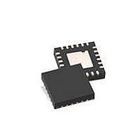
ISP1506ABS,518 NXP Semiconductors, ISP1506ABS,518 Datasheet - Page 63

ISP1506ABS,518
Manufacturer Part Number
ISP1506ABS,518
Description
RF Transceiver USB ULPI TRNSCVR
Manufacturer
NXP Semiconductors
Datasheet
1.ISP1506BBS557.pdf
(80 pages)
Specifications of ISP1506ABS,518
Number Of Transceivers
1
Esd Protection
YeskV
Operating Supply Voltage (typ)
Not RequiredV
Operating Temperature Classification
Industrial
Operating Supply Voltage (max)
Not RequiredV
Operating Supply Voltage (min)
Not RequiredV
Mounting
Surface Mount
Operating Temperature (max)
85C
Operating Temperature (min)
-40C
Operating Supply Voltage
1.65 V to 3.6 V
Mounting Style
SMD/SMT
Package / Case
HVQFN-24
Lead Free Status / RoHS Status
Compliant
Other names
935278332518 ISP1506ABS-T
NXP Semiconductors
Table 56.
V
ISP1506A_ISP1506B_2
Product data sheet
Symbol
t
t
t
t
Receiver timing
Differential receiver
t
t
PHZ
PLZ
PZH
PZL
PLH(rcv)
PHL(rcv)
CC
Fig 26. Rise time and fall time
Fig 28. Timing of TX_ENABLE to DP and DM
1.8 V
V
V
V
V
0 V
OH
OH
OL
= 3.0 V to 3.6 V; V
OL
logic
input
differential
data lines
0.9 V
Parameter
driver disable delay from
HIGH level
driver disable delay from
LOW level
driver enable delay to
HIGH level
driver enable delay to
LOW level
receiver propagation
delay (LOW to HIGH)
receiver propagation
delay (HIGH to LOW)
Dynamic characteristics: analog I/O pins (DP and DM)
t
HSR
10 %
15.1 ULPI timing
, t
FR
t
V
t
PZH
PZL
CRS
, t
LR
CC(I/O)
90 %
ULPI interface timing requirements are given in
synchronous mode only. All timing is measured with respect to the ISP1506 CLOCK pin.
All signals are clocked on the rising edge of CLOCK.
= 1.65 V to 1.95 V; T
V
V
OH
90 %
OL
+ 0.3 V
t
Conditions
TX_ENABLE to DP, DM;
see
TX_ENABLE to DP, DM;
see
TX_ENABLE to DP, DM;
see
TX_ENABLE to DP, DM;
see
DP, DM to DAT, SE0;
see
DP, DM to DAT, SE0;
see
0.3 V
HSF
t
t
PHZ
0.9 V
PLZ
10 %
, t
Figure 28
Figure 28
Figure 28
Figure 28
Figure 29
Figure 29
FF
, t
LF
Rev. 02 — 28 August 2008
amb
004aaa861
004aaa574
= 40 C to +85 C; unless otherwise specified.
Fig 27. Timing of DAT and SE0 when transmitting to
Fig 29. Timing of DAT and SE0 when receiving from
1.8 V
differential
data lines
V
V
0 V
logic input
OH
OL
logic output
0.8 V
2.0 V
V
V
differential
data lines
OH
…continued
OL
DP and DM
DP and DM
0.9 V
ISP1506A; ISP1506B
V
CRS
Figure
Min
-
-
-
-
-
-
t
PLH(drv)
V
t
PLH(rcv)
CRS
30. This timing applies to
0.9 V
ULPI HS USB OTG transceiver
Typ
-
-
-
-
-
-
Max
12
12
20
20
17
17
© NXP B.V. 2008. All rights reserved.
t
PHL(drv)
0.9 V
t
V
PHL(rcv)
CRS
V
004aaa985
004aaa573
CRS
Unit
ns
ns
ns
ns
ns
ns
0.9 V
62 of 79


