STK12C68-SF25 Cypress Semiconductor Corp, STK12C68-SF25 Datasheet - Page 3
STK12C68-SF25
Manufacturer Part Number
STK12C68-SF25
Description
STK12C68-SF25
Manufacturer
Cypress Semiconductor Corp
Datasheet
1.STK12C68-SF45TR.pdf
(23 pages)
Specifications of STK12C68-SF25
Format - Memory
RAM
Memory Type
NVSRAM (Non-Volatile SRAM)
Memory Size
64K (8K x 8)
Speed
25ns
Interface
Parallel
Voltage - Supply
4.5 V ~ 5.5 V
Operating Temperature
0°C ~ 70°C
Package / Case
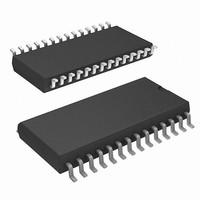
28-SOIC (8.69mm width)
Lead Free Status / RoHS Status
Lead free / RoHS Compliant


Pin Configurations
Pin Definitions
Document Number: 001-51027 Rev. *D
Pin Name
DQ
A
V
HSB
0
V
V
WE
CE
OE
0
–A
CAP
SS
CC
-DQ
12
7
Alt
W
G
E
Input or Output Bidirectional Data I/O Lines. Used as input or output lines depending on operation.
Input or Output Hardware Store Busy (HSB). When LOW, this output indicates a Hardware Store is in progress.
Power Supply Power Supply Inputs to the Device.
Power Supply AutoStore Capacitor. Supplies power to nvSRAM during power loss to store data from SRAM
I/O Type
Ground
Input
Input
Input
Input
Address Inputs. Used to select one of the 8,192 bytes of the nvSRAM.
Write Enable Input, Active LOW. When the chip is enabled and WE is LOW, data on the I/O
pins is written to the specific address location.
Chip Enable Input, Active LOW. When LOW, selects the chip. When HIGH, deselects the chip.
Output Enable, Active LOW. The active LOW OE input enables the data output buffers during
read cycles. Deasserting OE HIGH causes the I/O pins to tristate.
Ground for the Device. The device is connected to ground of the system.
When pulled low external to the chip, it initiates a nonvolatile STORE operation. A weak internal
pull up resistor keeps this pin high if not connected (connection optional).
to nonvolatile elements.
Figure 1. 28-Pin SOIC/DIP and LLC
Description
STK12C68
Page 3 of 23
[+] Feedback
Related parts for STK12C68-SF25
Image
Part Number
Description
Manufacturer
Datasheet
Request
R

Part Number:
Description:
STK12C68-5C35M
Manufacturer:
Cypress Semiconductor Corp
Datasheet:

Part Number:
Description:
STK12C68-SF25I
Manufacturer:
Cypress Semiconductor Corp
Datasheet:
Part Number:
Description:
IC NVSRAM 64KBIT 45NS 28SOIC
Manufacturer:
Cypress Semiconductor Corp
Datasheet:

Part Number:
Description:
Manufacturer:
Cypress Semiconductor Corp
Datasheet:
Part Number:
Description:
Manufacturer:
Cypress Semiconductor Corp
Datasheet:

Part Number:
Description:
Manufacturer:
Cypress Semiconductor Corp
Datasheet:
Part Number:
Description:
Manufacturer:
Cypress Semiconductor Corp
Datasheet:
Part Number:
Description:
Manufacturer:
Cypress Semiconductor Corp
Datasheet:
Part Number:
Description:
STK12C68-SF45
Manufacturer:
Cypress Semiconductor Corp
Datasheet:
Part Number:
Description:
STK12C68-5C55M
Manufacturer:
Cypress Semiconductor Corp
Datasheet:
Part Number:
Description:
STK12C68-5K35M
Manufacturer:
Cypress Semiconductor Corp
Datasheet:
Part Number:
Description:
STK12C68-5K55M
Manufacturer:
Cypress Semiconductor Corp
Datasheet:

Part Number:
Description:
STK12C68-5L35M
Manufacturer:
Cypress Semiconductor Corp
Datasheet:
Part Number:
Description:
STK12C68-5L55M
Manufacturer:
Cypress Semiconductor Corp
Datasheet:
Part Number:
Description:
STK12C68-C35I
Manufacturer:
Cypress Semiconductor Corp
Datasheet: