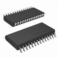
STK12C68-SF25 Cypress Semiconductor Corp, STK12C68-SF25 Datasheet - Page 12

STK12C68-SF25
Manufacturer Part Number
STK12C68-SF25
Description
STK12C68-SF25
Manufacturer
Cypress Semiconductor Corp
Datasheet
1.STK12C68-SF45TR.pdf
(23 pages)
Specifications of STK12C68-SF25
Format - Memory
RAM
Memory Type
NVSRAM (Non-Volatile SRAM)
Memory Size
64K (8K x 8)
Speed
25ns
Interface
Parallel
Voltage - Supply
4.5 V ~ 5.5 V
Operating Temperature
0°C ~ 70°C
Package / Case
28-SOIC (8.69mm width)
Lead Free Status / RoHS Status
Lead free / RoHS Compliant
Switching Waveforms
Notes
Document Number: 001-51027 Rev. *D
SRAM Write Cycle
t
t
t
t
t
t
t
t
t
t
10. If WE is Low when CE goes Low, the outputs remain in the high impedance state.
11. HSB must be high during SRAM Write cycles.
12. CE or WE must be greater than V
WC
PWE
SCE
SD
HD
AW
SA
HA
HZWE
LZWE
Parameter
Cypress
[9]
[9,10]
ADDRESS
DATA OUT
ADDRESS
DATA OUT
DATA IN
DATA IN
WE
CE
Parameter
CE
WE
t
t
t
t
t
t
t
t
t
t
AVAV
WLWH,
ELWH,
DVWH,
WHDX,
AVWH,
AVWL,
WHAX,
WLQZ
WHQX
t
t
t
t
t
t
t
AVEL
ELEH
AVEH
EHAX
WLEH
DVEH
EHDX
Alt
IH
during address transitions.
PREVIOUS DATA
t
SA
Figure 10. SRAM Write Cycle 2: CE Controlled
Figure 9. SRAM Write Cycle 1: WE Controlled
Write Cycle Time
Write Pulse Width
Chip Enable To End of Write
Data Setup to End of Write
Data Hold After End of Write
Address Setup to End of Write
Address Setup to Start of Write
Address Hold After End of Write
Write Enable to Output Disable
Output Active After End of Write
t
SA
Description
HIGH IMPEDANCE
t
t
AW
PWE
t
AW
t
HZWE
t
t
t
SCE
WC
SCE
t
WC
t
t
SD
HIGH IMPEDANCE
PWE
DATA VALID
DATA VALID
t
SD
Min
25
20
20
10
20
0
0
0
5
25 ns
Max
[11, 12]
[11, 12]
t
10
HA
t
t
t
HD
HD
HA
Min
35
25
25
12
25
0
0
0
5
t
35 ns
LZWE
Max
13
Min
45
30
30
15
30
0
0
0
5
STK12C68
45 ns
Page 12 of 23
Max
14
Unit
ns
ns
ns
ns
ns
ns
ns
ns
ns
ns
[+] Feedback


