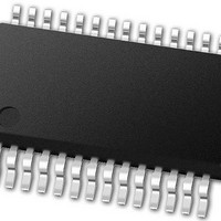
PIC24FJ32GA102-E/SS Microchip Technology, PIC24FJ32GA102-E/SS Datasheet - Page 165

PIC24FJ32GA102-E/SS
Manufacturer Part Number
PIC24FJ32GA102-E/SS
Description
16-bit, 16 MIPS, 32KB Flash, 8KB RAM, Nanowatt XLP 28 SSOP .209in TUBE
Manufacturer
Microchip Technology
Series
PIC® XLP™ 24Fr
Datasheet
1.PIC24FJ32GA102-ISP.pdf
(308 pages)
Specifications of PIC24FJ32GA102-E/SS
Processor Series
PIC24
Core
PIC24F
Data Bus Width
16 bit
Program Memory Type
Flash
Program Memory Size
32 KB
Data Ram Size
8192 B
Interface Type
I2C, SPI, UART
Maximum Clock Frequency
32 MHz
Number Of Programmable I/os
21
Number Of Timers
5
Operating Supply Voltage
2 V to 3.6 V
Maximum Operating Temperature
+ 125 C
Mounting Style
SMD/SMT
Package / Case
SSOP-28
Development Tools By Supplier
MPLAB Integrated Development Environment
Minimum Operating Temperature
- 40 C
Operating Temperature Range
- 40 C to + 125 C
Supply Current (max)
300 mA
Core Processor
PIC
Core Size
16-Bit
Speed
32MHz
Connectivity
I²C, IrDA, SPI, UART/USART
Peripherals
Brown-out Detect/Reset, LVD, POR, PWM, WDT
Number Of I /o
21
Eeprom Size
-
Ram Size
8K x 8
Voltage - Supply (vcc/vdd)
2 V ~ 3.6 V
Data Converters
A/D 10x10b
Oscillator Type
Internal
Operating Temperature
-40°C ~ 125°C
Lead Free Status / Rohs Status
Details
- Current page: 165 of 308
- Download datasheet (3Mb)
15.0
The Serial Peripheral Interface (SPI) module is a
synchronous serial interface useful for communicating
with other peripheral or microcontroller devices. These
peripheral devices may be serial EEPROMs, shift
registers, display drivers, A/D Converters, etc. The SPI
module is compatible with Motorola
interfaces. All devices of the PIC24FJ64GA104 family
include three SPI modules
The module supports operation in two buffer modes. In
Standard mode, data is shifted through a single serial
buffer. In Enhanced Buffer mode, data is shifted
through an 8-level FIFO buffer.
The module also supports a basic framed SPI protocol
while operating in either Master or Slave mode. A total
of four framed SPI configurations are supported.
2010 Microchip Technology Inc.
Note:
Note:
SERIAL PERIPHERAL
INTERFACE (SPI)
This data sheet summarizes the features
of this group of PIC24F devices. It is not
intended to be a comprehensive reference
source. For more information, refer to the
“PIC24F
Section 23. “Serial Peripheral Interface
(SPI)” (DS39699).
Do not perform read-modify-write opera-
tions (such as bit-oriented instructions) on
the SPIxBUF register in either Standard or
Enhanced Buffer mode.
Family
Reference
®
SPI and SIOP
Manual”,
PIC24FJ64GA104 FAMILY
The SPI serial interface consists of four pins:
• SDIx: Serial Data Input
• SDOx: Serial Data Output
• SCKx: Shift Clock Input or Output
• SSx: Active-Low Slave Select or Frame
The SPI module can be configured to operate using
2, 3 or 4 pins. In the 3-pin mode, SSx is not used. In the
2-pin mode, both SDOx and SSx are not used.
Block diagrams of the module in Standard and
Enhanced modes are shown in Figure 15-1 and
Figure 15-2.
Synchronization I/O Pulse
Note:
In this section, the SPI modules are
referred to together as SPIx or separately
as SPI1, SPI2 or SPI3. Special Function
Registers will follow a similar notation. For
example, SPIxCON1 and SPIxCON2 refer
to the control registers for any of the 3 SPI
modules.
DS39951C-page 165
Related parts for PIC24FJ32GA102-E/SS
Image
Part Number
Description
Manufacturer
Datasheet
Request
R

Part Number:
Description:
Manufacturer:
Microchip Technology Inc.
Datasheet:

Part Number:
Description:
Manufacturer:
Microchip Technology Inc.
Datasheet:

Part Number:
Description:
Manufacturer:
Microchip Technology Inc.
Datasheet:

Part Number:
Description:
Manufacturer:
Microchip Technology Inc.
Datasheet:

Part Number:
Description:
Manufacturer:
Microchip Technology Inc.
Datasheet:

Part Number:
Description:
Manufacturer:
Microchip Technology Inc.
Datasheet:

Part Number:
Description:
Manufacturer:
Microchip Technology Inc.
Datasheet:

Part Number:
Description:
Manufacturer:
Microchip Technology Inc.
Datasheet:


