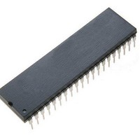
PIC16F1517-E/P Microchip Technology, PIC16F1517-E/P Datasheet - Page 143

PIC16F1517-E/P
Manufacturer Part Number
PIC16F1517-E/P
Description
40-pin, 14KB Flash, 512B RAM, 10-bit ADC, 2xCCP, SPI, MI2C, EUSART, 2.3V-5.5V 40
Manufacturer
Microchip Technology
Series
PIC® XLP™ 16Fr
Datasheet
1.PIC16F1516-EMV.pdf
(344 pages)
Specifications of PIC16F1517-E/P
Processor Series
PIC16F151x
Core
PIC
Data Bus Width
8 bit
Program Memory Type
Flash
Program Memory Size
8 KB
Data Ram Size
512 B
Interface Type
I2C, SPI, USART
Maximum Clock Frequency
20 MHz
Number Of Programmable I/os
36
Number Of Timers
3
Operating Supply Voltage
2.3 V to 5.5 V
Maximum Operating Temperature
+ 125 C
Mounting Style
Through Hole
Package / Case
PDIP-40
Core Processor
PIC
Core Size
8-Bit
Speed
20MHz
Connectivity
I²C, LIN, SPI, UART/USART
Peripherals
Brown-out Detect/Reset, POR, PWM, WDT
Number Of I /o
36
Eeprom Size
-
Ram Size
512 x 8
Voltage - Supply (vcc/vdd)
2.3 V ~ 5.5 V
Data Converters
A/D 28x10b
Oscillator Type
Internal
Operating Temperature
-40°C ~ 125°C
Lead Free Status / Rohs Status
Details
Available stocks
Company
Part Number
Manufacturer
Quantity
Price
Company:
Part Number:
PIC16F1517-E/PT
Manufacturer:
Microchip Technology
Quantity:
10 000
- Current page: 143 of 344
- Download datasheet (3Mb)
TABLE 16-1:
FIGURE 16-2:
2011 Microchip Technology Inc.
Legend: Shaded cells are outside of recommended range.
Note 1:
Clock Source
ADC Clock Period (T
Fosc/16
Fosc/32
Fosc/64
Fosc/2
Fosc/4
Fosc/8
ADC
F
2:
3:
4:
RC
T
Set GO bit
CY
Holding capacitor is disconnected from analog input (typically 100 ns)
The F
These values violate the minimum required T
For faster conversion times, the selection of another clock source is recommended.
The ADC clock period (T
derived from the system clock F
to be performed with the device in Sleep mode.
- T
AD
Conversion starts
RC
ADC CLOCK PERIOD (T
ADCS<2:0>
T
AD
source has a typical T
1 T
000
100
001
101
010
110
x11
ANALOG-TO-DIGITAL CONVERSION T
AD
AD
b9
)
2 T
AD
b8
1.0-6.0 s
3 T
AD
100 ns
200 ns
400 ns
20 MHz
800 ns
1.6 s
3.2 s
) and total ADC conversion time can be minimized when the ADC clock is
AD
b7
4 T
AD
(2)
(2)
(2)
OSC
(1,4)
time of 1.6 s for V
AD
AD
. However, the F
b6
5 T
) V
On the following cycle:
ADRESH:ADRESL is loaded, GO bit is cleared,
ADIF bit is set, holding capacitor is connected to analog input.
Preliminary
1.0-6.0 s
S
AD
125 ns
250 ns
b5
. DEVICE OPERATING FREQUENCIES
0.5 s
16 MHz
1.0 s
2.0 s
4.0 s
6 T
AD
time.
AD
(2)
b4
(2)
(2)
(1,4)
Device Frequency (F
7 T
RC
DD
PIC16(L)F1516/7/8/9
AD
b3
clock source must be used when conversions are
.
1.0-6.0 s
AD
8
250 ns
500 ns
8.0 s
8 MHz
CYCLES
1.0 s
2.0 s
4.0 s
T
AD
b2
9 T
(3)
(2)
(2)
(1,4)
AD
b1
10
OSC
T
1.0-6.0 s
AD
b0
16.0 s
500 ns
)
8.0 s
11
4 MHz
1.0 s
2.0 s
4.0 s
(3)
(2)
(3)
(1,4)
DS41452B-page 143
1.0-6.0 s
16.0 s
32.0 s
64.0 s
8.0 s
1 MHz
2.0 s
4.0 s
(3)
(3)
(3)
(3)
(1,4)
Related parts for PIC16F1517-E/P
Image
Part Number
Description
Manufacturer
Datasheet
Request
R

Part Number:
Description:
IC, 8BIT MCU, PIC16F, 32MHZ, SOIC-18
Manufacturer:
Microchip Technology
Datasheet:

Part Number:
Description:
IC, 8BIT MCU, PIC16F, 32MHZ, SSOP-20
Manufacturer:
Microchip Technology
Datasheet:

Part Number:
Description:
IC, 8BIT MCU, PIC16F, 32MHZ, DIP-18
Manufacturer:
Microchip Technology
Datasheet:

Part Number:
Description:
IC, 8BIT MCU, PIC16F, 32MHZ, QFN-28
Manufacturer:
Microchip Technology
Datasheet:

Part Number:
Description:
IC, 8BIT MCU, PIC16F, 32MHZ, QFN-28
Manufacturer:
Microchip Technology
Datasheet:

Part Number:
Description:
IC, 8BIT MCU, PIC16F, 32MHZ, QFN-28
Manufacturer:
Microchip Technology
Datasheet:

Part Number:
Description:
IC, 8BIT MCU, PIC16F, 32MHZ, SSOP-20
Manufacturer:
Microchip Technology
Datasheet:

Part Number:
Description:
IC, 8BIT MCU, PIC16F, 20MHZ, DIP-40
Manufacturer:
Microchip Technology
Datasheet:

Part Number:
Description:
IC, 8BIT MCU, PIC16F, 32MHZ, QFN-28
Manufacturer:
Microchip Technology
Datasheet:

Part Number:
Description:
IC, 8BIT MCU, PIC16F, 20MHZ, MQFP-44
Manufacturer:
Microchip Technology
Datasheet:

Part Number:
Description:
IC, 8BIT MCU, PIC16F, 20MHZ, QFN-20
Manufacturer:
Microchip Technology
Datasheet:

Part Number:
Description:
IC, 8BIT MCU, PIC16F, 32MHZ, QFN-28
Manufacturer:
Microchip Technology
Datasheet:

Part Number:
Description:
MCU 14KB FLASH 768B RAM 64-TQFP
Manufacturer:
Microchip Technology
Datasheet:

Part Number:
Description:
7 KB Flash, 384 Bytes RAM, 32 MHz Int. Osc, 16 I/0, Enhanced Mid Range Core, Low
Manufacturer:
Microchip Technology

Part Number:
Description:
14KB Flash, 512B RAM, 256B EEPROM, LCD, 1.8-5.5V 40 UQFN 5x5x0.5mm TUBE
Manufacturer:
Microchip Technology
Datasheet:


