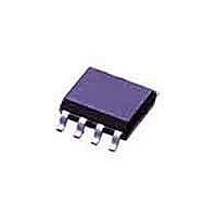
PIC12LF1840-E/SN Microchip Technology, PIC12LF1840-E/SN Datasheet - Page 313

PIC12LF1840-E/SN
Manufacturer Part Number
PIC12LF1840-E/SN
Description
7 KB Flash, 256 Bytes RAM, 32 MHz Int. Osc, 6 I/0, Enhanced Mid Range Core, Nano
Manufacturer
Microchip Technology
Series
PIC® XLP™ 12Fr
Datasheet
1.PIC12F1840-EMF.pdf
(382 pages)
Specifications of PIC12LF1840-E/SN
Processor Series
PIC12F
Core
PIC
Program Memory Type
Flash
Program Memory Size
7 KB
Data Ram Size
256 B
Interface Type
MI2C, SPI, EUSART
Number Of Timers
3
Operating Supply Voltage
1.8 V to 5.5 V
Maximum Operating Temperature
+ 125 C
Mounting Style
SMD/SMT
Package / Case
SOIC-8
Development Tools By Supplier
MPLAB IDE Software
Minimum Operating Temperature
- 40 C
Core Processor
RISC
Core Size
8-Bit
Speed
32MHz
Connectivity
I²C, LIN, SPI, UART/USART
Peripherals
Brown-out Detect/Reset, POR, PWM, WDT
Number Of I /o
5
Eeprom Size
256 x 8
Ram Size
256 x 8
Voltage - Supply (vcc/vdd)
1.8 V ~ 3.6 V
Data Converters
A/D 4x10b
Oscillator Type
Internal
Operating Temperature
-40°C ~ 125°C
Lead Free Status / Rohs Status
Details
Available stocks
Company
Part Number
Manufacturer
Quantity
Price
Company:
Part Number:
PIC12LF1840-E/SN
Manufacturer:
MICRON
Quantity:
4 500
- Current page: 313 of 382
- Download datasheet (4Mb)
CALL
Syntax:
Operands:
Operation:
Status Affected:
Description:
CALLW
Syntax:
Operands:
Operation:
Status Affected:
Description:
CLRF
Syntax:
Operands:
Operation:
Status Affected:
Description:
CLRW
Syntax:
Operands:
Operation:
Status Affected:
Description:
2011 Microchip Technology Inc.
Call Subroutine
[ label ] CALL k
0 k 2047
(PC)+ 1 TOS,
k PC<10:0>,
(PCLATH<6:3>) PC<14:11>
None
Call Subroutine. First, return address
(PC + 1) is pushed onto the stack.
The eleven-bit immediate address is
loaded into PC bits <10:0>. The upper
bits of the PC are loaded from
PCLATH. CALL is a two-cycle instruc-
tion.
Clear W
[ label ] CLRW
None
00h (W)
1 Z
Z
W register is cleared. Zero bit (Z) is
set.
[ label ] CALLW
(PC) +1 TOS,
(W) PC<7:0>,
(PCLATH<6:0>) PC<14:8>
Subroutine call with W. First, the
return address (PC + 1) is pushed
onto the return stack. Then, the con-
tents of W is loaded into PC<7:0>,
and the contents of PCLATH into
PC<14:8>. CALLW is a two-cycle
instruction.
Subroutine Call With W
None
None
Clear f
[ label ] CLRF
0 f 127
00h (f)
1 Z
Z
The contents of register ‘f’ are cleared
and the Z bit is set.
f
Preliminary
CLRWDT
Syntax:
Operands:
Operation:
Status Affected:
Description:
COMF
Syntax:
Operands:
Operation:
Status Affected:
Description:
DECF
Syntax:
Operands:
Operation:
Status Affected:
Description:
PIC12(L)F1840
Complement f
[ label ] COMF
0 f 127
d [0,1]
(f) (destination)
Z
The contents of register ‘f’ are com-
plemented. If ‘d’ is ‘0’, the result is
stored in W. If ‘d’ is ‘1’, the result is
stored back in register ‘f’.
Decrement f
[ label ] DECF f,d
0 f 127
d [0,1]
(f) - 1 (destination)
Z
result is stored in the W
register. If ‘d’ is ‘1’, the result is stored
back in register ‘f’.
Clear Watchdog Timer
[ label ] CLRWDT
None
00h WDT
0 WDT prescaler,
1 TO
1 PD
TO, PD
CLRWDT instruction resets the Watch-
dog Timer. It also resets the prescaler
of the WDT.
Status bits TO and PD are set.
Decrement register ‘f’. If ‘d’ is ‘0’, the
f,d
DS41441B-page 313
Related parts for PIC12LF1840-E/SN
Image
Part Number
Description
Manufacturer
Datasheet
Request
R

Part Number:
Description:
Manufacturer:
Microchip Technology Inc.
Datasheet:

Part Number:
Description:
Manufacturer:
Microchip Technology Inc.
Datasheet:

Part Number:
Description:
Manufacturer:
Microchip Technology Inc.
Datasheet:

Part Number:
Description:
Manufacturer:
Microchip Technology Inc.
Datasheet:

Part Number:
Description:
Manufacturer:
Microchip Technology Inc.
Datasheet:

Part Number:
Description:
Manufacturer:
Microchip Technology Inc.
Datasheet:

Part Number:
Description:
Manufacturer:
Microchip Technology Inc.
Datasheet:

Part Number:
Description:
Manufacturer:
Microchip Technology Inc.
Datasheet:


