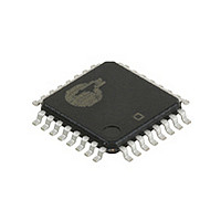
CY2DP3110AI Cypress Semiconductor Corp, CY2DP3110AI Datasheet - Page 3

CY2DP3110AI
Manufacturer Part Number
CY2DP3110AI
Description
Manufacturer
Cypress Semiconductor Corp
Type
Clock Driverr
Datasheet
1.CY2DP3110AI.pdf
(10 pages)
Specifications of CY2DP3110AI
Number Of Clock Inputs
2
Mode Of Operation
Differential
Output Frequency
1500MHz
Output Logic Level
ECL/PECL
Operating Supply Voltage (min)
-2.375/2.375V
Operating Supply Voltage (typ)
-2.5/-3.3/2.5/3.3V
Operating Supply Voltage (max)
-3.465/3.465V
Package Type
TQFP
Operating Temp Range
-40C to 85C
Operating Temperature Classification
Industrial
Signal Type
ECL/HSTL/PECL
Mounting
Surface Mount
Pin Count
32
Lead Free Status / RoHS Status
Not Compliant
Available stocks
Company
Part Number
Manufacturer
Quantity
Price
Company:
Part Number:
CY2DP3110AI
Manufacturer:
ATHEROS
Quantity:
40
Document #: 38-07469 Rev. *I
Absolute Maximum Ratings
Operating Conditions
PECL/HSTL DC Electrical Specifications
V
V
T
T
ESD
M
Gate Count Total Number of Used Gates
Multiple Supplies: The Voltage on any input or I/O pin cannot exceed the power pin during power-up. Power supply sequencing is NOT required.
I
LU
T
Ø
Ø
I
C
L
V
V
V
I
V
V
V
V
V
V
V
V
Notes:
10. Equivalent to a termination of 50Ω to VTT. I
11. V
BB
EE
IN
Parameter
Parameter
4. Theta JA EIA JEDEC 51 test board conditions (typical value); Theta JC 883E Method 1012.1
5. Power Calculation: V
6. where V
7. Inputs have internal pull-up/pull-down or biasing resistors which affect the input current.
8. Refer to Figure 1.
9. V
Parameter
A
S
J
IN
CC
EE
IN
TT
OUT
CC
CMR
X
OH
OL
IH
IL
BB
IN
Jc
Ja
SL
I
swing lies within the V
[3]
X
IL
h
(AC) is the crosspoint of the differential HSTL input signal. Normal AC operation is obtained when the crosspoint is within the V
will operate down to V
CC
is 3.3V±5% or 2.5V±5%.
Positive Supply Voltage
Negative Supply Voltage
Temperature, Storage
Temperature, Junction
ESD Protection
Moisture Sensitivity Level
Output Reference Current
Latch Up Immunity
Temperature, Operating Ambient
Dissipation, Junction to Case
Dissipation, Junction to Ambient
Maximum Quiescent Supply Current
Input pin capacitance
Pin Inductance
Input Voltage
Output Termination Voltage
Output Voltage
Input Current
Operating Voltage
PECL Input Differential Cross Point
Voltage
HSTL Input Differential Crosspoint Volt-
age
Output High Voltage
Output Low Voltage
V
V
Input Voltage, High
Input Voltage, Low
Output Reference Voltage
CC
CC
[9]
= 3.3V ± 5%
= 2.5V ± 5%
CC
DIF
[8]
* I
(AC) specification. Violation of V
EE
EE
; V
+0.5 (I
[7]
IH
Description
Description
Description
will operate up to V
OH
+ I
OL
OHMIN
) (V
OH
=(V
– V
CC
OHMIN
OL
.
X
) (number of differential outputs used); I
(AC) or V
– V
TT
)/50; I
Non-Functional
Non-Functional
Relative to V
Functional
Functional
V
Non-Functional
Non-Functional
Human Body Model
Assembled Die
Functional, typical
Functional
Relative to V
Relative to V
Relative to V
V
DIF
2.5V ± 5%, V
3.3V ± 5%, V
Differential operation
Standard Load Differential
Operation
I
I
Single-ended operation
Single-ended operation
Relative to V
OH
OL
EE
IN
(AC) impacts the device propagation delay, device and part-to-part skew. Refer to Figure 2.
OHMAX
= V
= –5 mA
= –30 mA
pin
IL
, or V
Condition
=(V
Condition
Condition
OHMAX
[10]
BB
CC
CC
CC
CC
EE
EE
[10]
IN
[6]
[6]
[6]
[6]
= V
= 0.0V
= 0.0V
– V
TT
IH
)/50; I
EE
does not include current going off chip.
OLMIN
V
=(V
V
V
CC
V
V
V
CC
CC
CC
CC
OLMIN
CC
2.375
3.135
– 1.945
Min.
0.68
1.2
– 1.995
– 1.165
– 1.620
Min.
Min.
–1.995
–0.3
–0.3
–0.3
-4.6
– 1.25
–65
–40
– V
FastEdge™ Series
TT
[11]
V
)/50; I
2000
35
76
CC
100
50
3
[4]
[4]
V
OLMAX
– 2
CC
V
V
X
V
V
V
V
V
CC
CC
(AC) range and the input
CY2DP3110
CC
CC
CC
CC
CC
130
2.625
3.465
– 0.880
=(V
Max.
+150
Max.
|200|
Max.
l150l
V
150
+85
4.6
0.3
0.9
– 1.625
– 1.220
3
1
CC
– 0.7
– 1.5
– 1.3
+ 0.3
+ 0.3
OLMAX
[5]
Page 3 of 10
[11]
– V
TT
gates
°C/W
°C/W
)/50.
Unit
N.A.
Unit
Unit
mA
mA
nH
uA
pF
uA
°C
°C
°C
V
V
V
V
V
V
V
V
V
V
V
V
V
V
V
V


