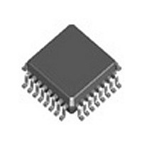
MC100ES6254FA IDT, Integrated Device Technology Inc, MC100ES6254FA Datasheet - Page 5

MC100ES6254FA
Manufacturer Part Number
MC100ES6254FA
Description
Manufacturer
IDT, Integrated Device Technology Inc
Type
Clock Driverr
Datasheet
1.MC100ES6254FA.pdf
(9 pages)
Specifications of MC100ES6254FA
Number Of Clock Inputs
2
Mode Of Operation
Differential
Output Frequency
3000MHz
Output Logic Level
LVPECL
Operating Supply Voltage (min)
2.375V
Operating Supply Voltage (typ)
2.5/3.3V
Operating Supply Voltage (max)
3.465V
Package Type
LQFP
Operating Temp Range
0C to 110C
Operating Temperature Classification
Commercial
Signal Type
LVPECL
Mounting
Surface Mount
Pin Count
32
Quiescent Current
85mA
Lead Free Status / RoHS Status
Not Compliant
Available stocks
Company
Part Number
Manufacturer
Quantity
Price
Company:
Part Number:
MC100ES6254FA
Manufacturer:
PREWELL
Quantity:
5 000
Company:
Part Number:
MC100ES6254FA
Manufacturer:
Freescale Semiconductor
Quantity:
10 000
IDT™ 2.5/3.3V Differential LVPECL 2x2 Clock Switch and Fanout Buffer
Freescale Timing Solutions Organization has been acquired by Integrated Device Technology, Inc
MC100ES6254
2.5/3.3V Differential LVPECL 2x2 Clock Switch and Fanout Buffer
a.
b.
c.
d.
e.
f.
g.
Table 7. AC CHARACTERISTICS (V
TIMING SOLUTIONS
Symbol
V
t
t
V
JIT(CC)
t
t
t
sk(PP)
DC
t
f
SK(P)
V
O(P-P)
sk(O)
PLDg
t
t
PDLf
CLK
CMR
r
AC characteristics apply for parallel output termination of 50 Ω to V
V
V
and the input swing lies within the V
part-to-part skew.
The MC100ES6254 is fully operational up to 3.0 GHz and is characterized up to 2.7 GHz.
Output pulse skew is the absolute difference of the propagation delay times: | t
Propagation delay OE deassertion to differential output disabled (differential low: true output low, complementary output high).
Propagation delay OE assertion to output enabled (active).
PD
PP
, t
CLKX
CLKX
PP
CMR
O
f
OEX
Qx[]
Qx[]
is the minimum differential input voltage swing required to maintain AC characteristics including tpd and device-to-device skew.
(AC) is the crosspoint of the differential input signal. Normal AC operation is obtained when the crosspoint is within the V
Differential input voltageb (peak-to-peak)
Differential input crosspoint voltage
Differential output voltage (peak-to-peak)
Input Frequency
Propagation delay CLK, 1 to QA[] or QB[]
Output-to-output skew
Output-to-output skew(part-to-part)
Output pulse skewe
Output duty cycle
Output cycle-to-cycle jitter
Output Rise/Fall Time
Output disable time
Output enable time
50%
Pulse Generator
Differential
Z = 50 Ω
t
PDL
Characteristics
(OEX to Qx[])
Freescale Semiconductor, Inc.
PP
Figure 3. MC100ES6254 output disable/enable timing
CC
For More Information On This Product,
(AC) specification. Violation of V
t
RMS (1 σ)
t
f
f
f
REF
REF
= 3.3 V ± 5% or 2.5 V ± 5%, T
O
O
O
R
Z
Figure 4. MC100ES6254 AC test reference
c
< 1.1 GHz
< 2.5 GHz
< 3.0 GHz
O
T
V
< 800 MHz
= 50 Ω
< 100 MHz
= 50 Ω
TT
MC100ES62
2.5⋅T + t
5
3⋅T + t
TT
DUT
0.45
0.35
0.20
49.4
45.2
0.05
.
Min
360
0.3
1.2
0
CMR
Outputs disabled
PD
PD
J
(AC) or V
= 0° to +110°C)
t
PLD
PLH
(OEX to Qx[])
Z
- t
R
O
T
PP
PHL
= 50 Ω
= 50 Ω
0.55
0.35
Typ
485
0.7
(AC) impacts the device propagation delay, device and
|.
a
3.5⋅T + t
4⋅T + t
V
3000
CC
Max
50.6
54.8
610
250
300
1.3
50
60
1
V
-0.3
TT
d
PD
PD
MHz
Unit
ps
ps
ps
ps
ps
ps
ns
ns
%
%
V
V
V
V
V
MC100ES6254/D
T = CLK period
T = CLK period
CMR
SEL0 ≠ SEL1
DC
DC
20% to 80%
MC100ES6254
Differential
Differential
Differential
Condition
NETCOM
fref
fref
(AC) range
= 50%
= 50%
5


