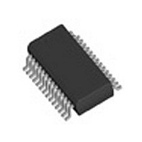
9179BF-03 IDT, Integrated Device Technology Inc, 9179BF-03 Datasheet - Page 3

9179BF-03
Manufacturer Part Number
9179BF-03
Description
Manufacturer
IDT, Integrated Device Technology Inc
Datasheet
1.9179BF-03.pdf
(11 pages)
Specifications of 9179BF-03
Number Of Outputs
10
Operating Supply Voltage (max)
3.465V
Operating Temp Range
0C to 70C
Propagation Delay Time
8ns
Operating Supply Voltage (min)
3.135V
Mounting
Surface Mount
Pin Count
28
Operating Supply Voltage (typ)
3.3V
Package Type
SSOP
Input Frequency
133MHz
Duty Cycle
55%
Operating Temperature Classification
Commercial
Lead Free Status / RoHS Status
Not Compliant
Available stocks
Company
Part Number
Manufacturer
Quantity
Price
Part Number:
9179BF-03LF
Manufacturer:
INTEGRATES
Quantity:
20 000
0258K 12/15/08
Technical Pin Function Descriptions
VDD
This is the power supply to the internal core logic of the
device as well as the clock output buffers for OUTPUT (0:9).
This pin operates at 3.3V volts. Clocks from the listed buffers
that it supplies will have a voltage swing from Ground to this
level. For the actual guaranteed high and low voltage levels
for the Clocks, please consult the DC parameter table in this
data sheet.
GND
This is the power supply ground (common or negative) return
pin for the internal core logic and all the output buffers.
OUTPUT (0:9)
These Output Clocks are use to drive Dynamic RAM’s and
are low skew copies of the CPU Clocks. The voltage swing of
the OUTPUTs output is controlled by the supply voltage
that is applied to VDD of the device, operates at 3.3 volts.
I
The SDATA and SCLOCK Inputs are use to program the
device. The clock generator is a slave-receiver device in the
I
configuration map for register functions. The I
in Philips I
followed.
BUF_IN
Input for Fanout buffers (OUTPUT 0:9).
OE
OE tristates all outputs when held low.
VDD1
This is the power supply to I
2
2
C
C protocol. It will allow read-back of the registers. See
2
C Peripherals Data Handbook (1996) should be
2
C circuitry.
2
C specification
3
ICS9179-03


